SNVSAX4 June 2017 LM1086-MIL
PRODUCTION DATA.
- 1 Features
- 2 Applications
- 3 Description
- 4 Revision History
- 5 Pin Configuration and Functions
- 6 Specifications
- 7 Detailed Description
-
8 Application and Implementation
- 8.1 Application Information
- 8.2 Typical Applications
- 8.3
Other Applications
- 8.3.1 Adjustable at 5 V
- 8.3.2 5-V Regulator with Shutdown
- 8.3.3 Battery Charger
- 8.3.4 Adjustable Fixed Regulator
- 8.3.5 Regulator With Reference
- 8.3.6 High-Current Lamp-Driver Protection
- 8.3.7 Battery-Backup-Regulated Supply
- 8.3.8 Ripple Rejection Enhancement
- 8.3.9 Automatic Light Control
- 8.3.10 Remote Sensing
- 9 Power Supply Recommendations
- 10Layout
- 11Device and Documentation Support
- 12Mechanical, Packaging, and Orderable Information
Package Options
Mechanical Data (Package|Pins)
- Y|0
Thermal pad, mechanical data (Package|Pins)
Orderable Information
5 Pin Configuration and Functions
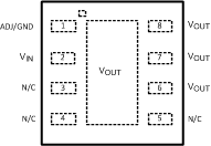
NGN Package
8-Pin WSON
Top View

NDE Package
3-Pin TO-220
Top View

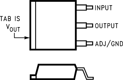
KTT Package
3-Pin DDPAK/TO-263
Top View

Pin Functions
| PIN | I/O | DESCRIPTION | ||
|---|---|---|---|---|
| NAME | NUMBER | |||
| KTT/NDE | NGN | |||
| ADJ/GND | 1 | 1 | –– | Adjust pin for the adjustable output voltage version. Ground pin for the fixed output voltage versions. |
| VIN | 3 | 2 | I | Input voltage pin for the regulator. |
| VOUT | 2, TAB | 6, 7, 8, PAD | O | Output voltage pin for the regulator. |
| N/C | 3, 4, 5 | –– | No connection | |