SNVS039J June 2000 – April 2015 LM1086
PRODUCTION DATA.
- 1 Features
- 2 Applications
- 3 Description
- 4 Revision History
- 5 Pin Configuration and Functions
- 6 Specifications
- 7 Detailed Description
-
8 Application and Implementation
- 8.1 Application Information
- 8.2
Typical Applications
- 8.2.1 1.2-V to 15-V Adjustable Regulator
- 8.2.2 Adjustable at 5 V
- 8.2.3 5-V Regulator with Shutdown
- 8.2.4 Battery Charger
- 8.2.5 Adjustable Fixed Regulator
- 8.2.6 Regulator With Reference
- 8.2.7 High Current Lamp Driver Protection
- 8.2.8 Battery Backup Regulated Supply
- 8.2.9 Ripple Rejection Enhancement
- 8.2.10 Automatic Light Control
- 8.2.11 Remote Sensing
- 9 Power Supply Recommendations
- 10Layout
- 11Device and Documentation Support
- 12Mechanical, Packaging, and Orderable Information
Package Options
Mechanical Data (Package|Pins)
Thermal pad, mechanical data (Package|Pins)
- KTT|3
Orderable Information
7.4.1 Output Voltage
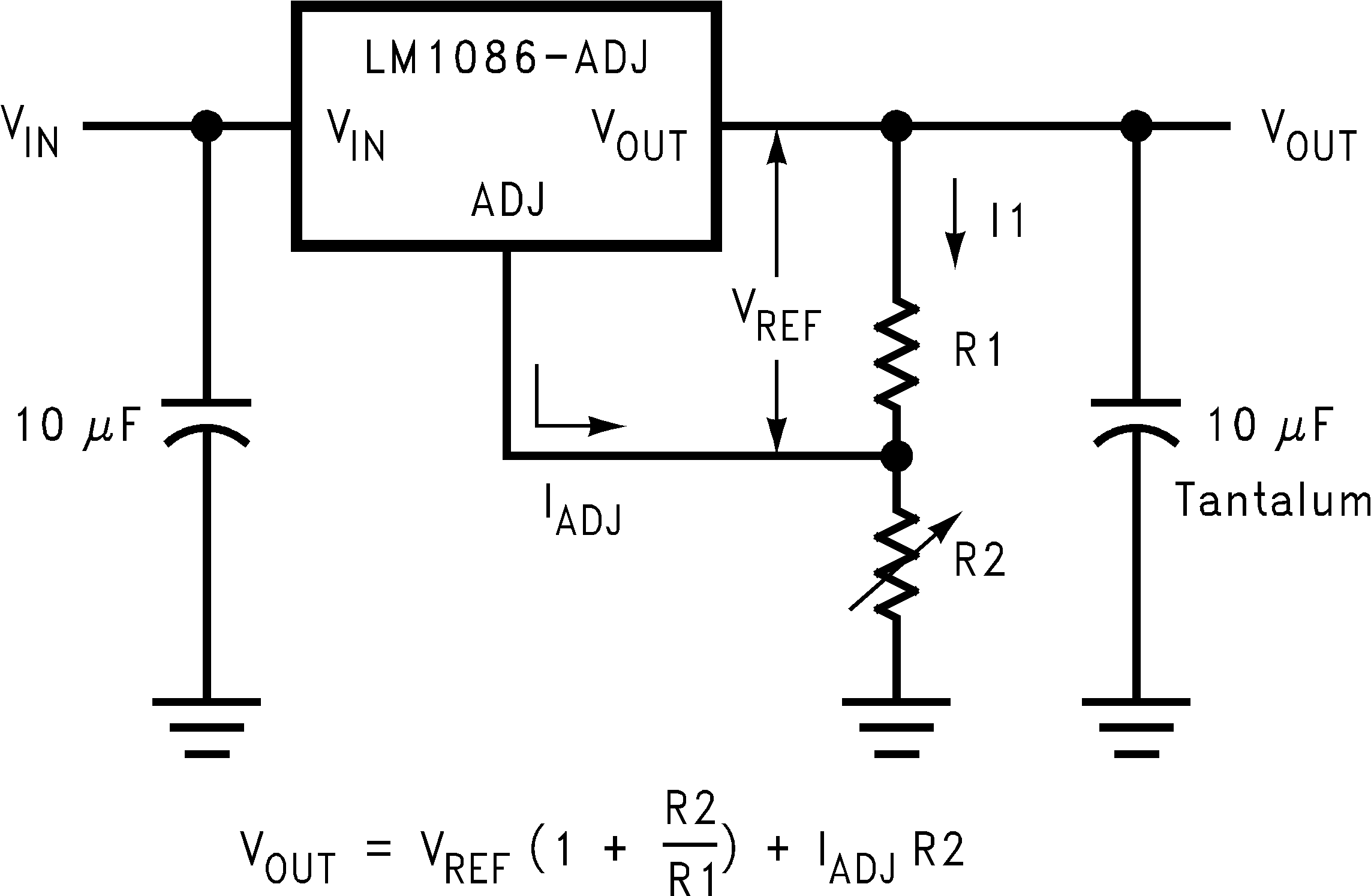
The LM1086 adjustable version develops a 1.25-V reference voltage, (VREF), between the output and the adjust terminal. As shown in Figure 16, this voltage is applied across resistor R1 to generate a constant current I1. This constant current then flows through R2. The resulting voltage drop across R2 adds to the reference voltage to sets the desired output voltage.
The current IADJ from the adjustment terminal introduces an output error . But since it is small (120uA max), it becomes negligible when R1 is in the 100 Ω range.
For fixed voltage devices, R1 and R2 are integrated inside the devices.
 Figure 16. Basic Adjustable Regulator