SLCS007K September 1973 – March 2017 LM111 , LM211 , LM311
PRODUCTION DATA.
- 1 Features
- 2 Applications
- 3 Description
- 4 Revision History
- 5 Pin Configuration and Functions
- 6 Specifications
- 7 Parameter Measurement Information
- 8 Detailed Description
- 9 Application and Implementation
- 10Power Supply Recommendations
- 11Layout
- 12Device and Documentation Support
- 13Mechanical, Packaging, and Orderable Information
Package Options
Refer to the PDF data sheet for device specific package drawings
Mechanical Data (Package|Pins)
- FK|20
- JG|8
Thermal pad, mechanical data (Package|Pins)
Orderable Information
5 Pin Configuration and Functions
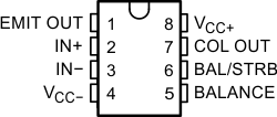
LMx11 D, JG, P, PS, or PW Package
8-Pin SOIC, CDIP, PDIP, SO or TSSOP
Top View

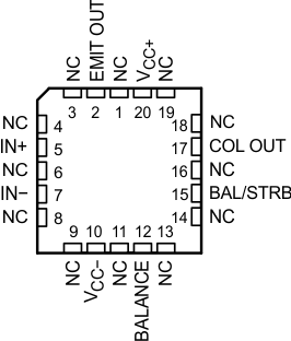
LM111 FK Package
20-Pin LCCC(1)
Top View

(1) NC = No internal connection
Pin Functions
| PIN | I/O(1) | DESCRIPTION | ||||
|---|---|---|---|---|---|---|
| NAME | LM211, LM311 | LM311 | LM111 | LM111 | ||
| SOIC, PDIP, TSSOP | SO | CDIP | LCCC | |||
| IN+ | 2 | 2 | 2 | 5 | I | Noninverting comparator |
| IN– | 3 | 3 | 3 | 7 | I | Inverting input comparator |
| BALANCE | 5 | 5 | 5 | 12 | I | Balance |
| BAL/STRB | 6 | 6 | 6 | 15 | I | Strobe |
| COL OUT | 7 | 7 | 7 | 17 | O | Output collector comparator |
| EMIT OUT | 1 | 1 | 1 | 2 | O | Output emitter comparator |
| VCC– | 4 | 4 | 4 | 10 | — | Negative supply |
| VCC+ | 8 | 8 | 8 | 20 | — | Positive supply |
| NC | — | — | — | 1 | — | No connect (No internal connection) |
| 3 | ||||||
| 4 | ||||||
| 6 | ||||||
| 8 | ||||||
| 9 | ||||||
| 11 | ||||||
| 13 | ||||||
| 14 | ||||||
| 16 | ||||||
| 18 | ||||||
| 19 | ||||||
(1) I = Input, O = Output