SNVS774Q May 2004 – June 2020 LM117 , LM317-N
PRODUCTION DATA.
- 1 Features
- 2 Applications
- 3 Description
- 4 Revision History
- 5 Device Comparison Table
- 6 Pin Configuration and Functions
- 7 Specifications
- 8 Detailed Description
-
9 Application and Implementation
- 9.1 Application Information
- 9.2
Typical Applications
- 9.2.1 1.25-V to 25-V Adjustable Regulator
- 9.2.2 5-V Logic Regulator With Electronic Shutdown
- 9.2.3 Slow Turnon 15-V Regulator
- 9.2.4 Adjustable Regulator With Improved Ripple Rejection
- 9.2.5 High Stability 10-V Regulator
- 9.2.6 High-Current Adjustable Regulator
- 9.2.7 Emitter-Follower Current Amplifier
- 9.2.8 1-A Current Regulator
- 9.2.9 Common-Emitter Amplifier
- 9.2.10 Low-Cost 3-A Switching Regulator
- 9.2.11 Current-Limited Voltage Regulator
- 9.2.12 Adjusting Multiple On-Card Regulators With Single Control
- 9.2.13 AC Voltage Regulator
- 9.2.14 12-V Battery Charger
- 9.2.15 Adjustable 4-A Regulator
- 9.2.16 Current-Limited 6-V Charger
- 9.2.17 Digitally Selected Outputs
- 10Power Supply Recommendations
- 11Layout
- 12Device and Documentation Support
- 13Mechanical, Packaging, and Orderable Information
Package Options
Mechanical Data (Package|Pins)
Thermal pad, mechanical data (Package|Pins)
Orderable Information
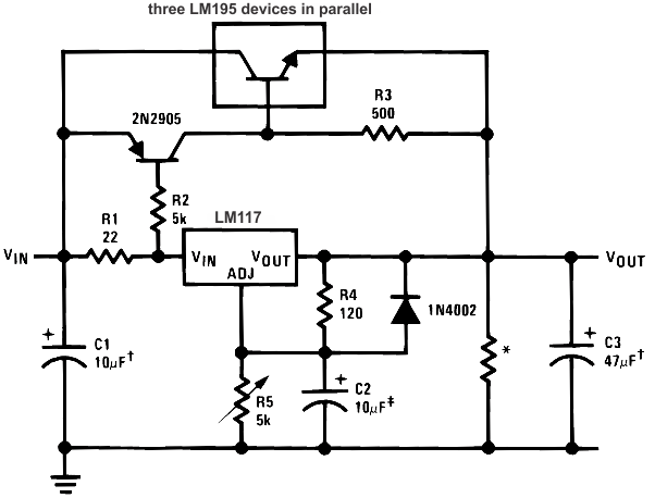
9.2.6 High-Current Adjustable Regulator
Using the LM195 power transistor in parallel with the LM117 can increase the maximum possible output load current (see Figure 24). Sense resistor R1 provides the 0.6 V across base to emitter to turn on the PNP. This on switch allows current to flow, and the voltage drop across R3 drives three LM195 power transistors designed to carry an excess of 1 A each.
NOTE
The selection of R1 determines a minimum load current for the PNP to turn on. The higher the resistor value, the lower the load current must be before the transistors turn on.

NOTE:
‡Optional—improves ripple rejection†Solid tantalum
*Minimum load current = 30 mA