SNVSC25 October 2021 LM117HVQML-SP
PRODUCTION DATA
- 1 Features
- 2 Applications
- 3 Description
- 4 Revision History
- 5 Related Products
- 6 Pin Configurations and Functions
- 7 Specifications
- 8 Detailed Description
- 9 Application and Implementation
- 10Power Supply Recommendations
- 11Layout
- 12Device and Documentation Support
- 13Mechanical, Packaging, and Orderable Information
Package Options
Mechanical Data (Package|Pins)
Thermal pad, mechanical data (Package|Pins)
Orderable Information
8.3.2 Load Regulation
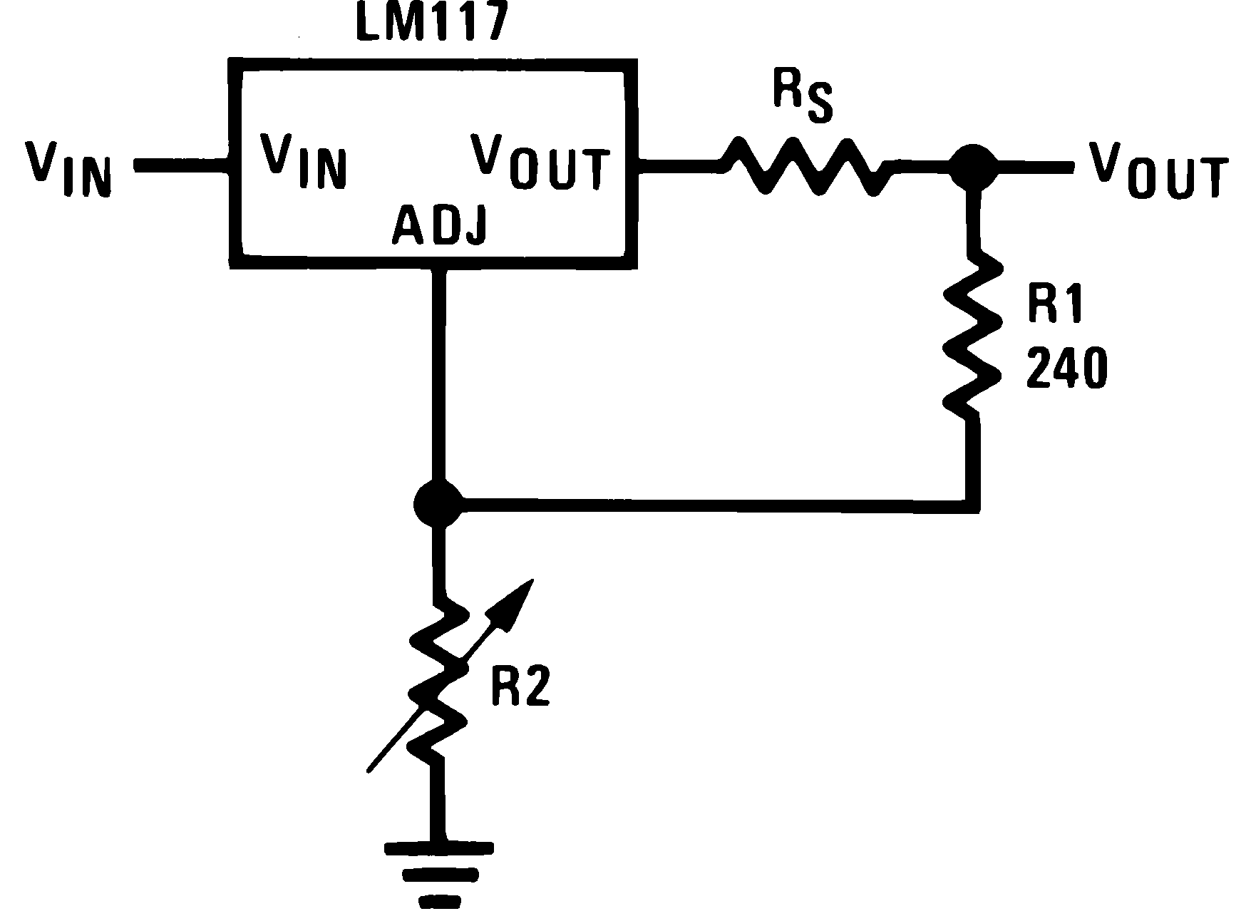
The LM117HVQML-SP is capable of providing extremely good load regulation but a few precautions are needed to obtain maximum performance. The current set resistor connected between the adjustment terminal and the output terminal (usually 240 Ω) should be tied directly to the output (case) of the regulator rather than near the load. This eliminates line drops from appearing effectively in series with the reference and degrading regulation. For example, a 15-V regulator with 0.05-Ω resistance between the regulator and load will have a load regulation due to line resistance of 0.05 Ω × IL. If the set resistor is connected near the load the effective line resistance will be 0.05 Ω (1 + R2 / R1) or in this case, 11.5 times worse.
Figure 8-1 shows the effect of resistance between the regulator and 240-Ω set resistor.
 Figure 8-1 Regulator With Line Resistance in Output
Lead
Figure 8-1 Regulator With Line Resistance in Output
LeadWith the TO-39 package, care should be taken to minimize the wire length of the output lead. The ground of R2 can be returned near the ground of the load to provide remote ground sensing and improve load regulation.