SNOSBJ3E November 1999 – December 2014 LM139-N , LM239-N , LM2901-N , LM339-N
PRODUCTION DATA.
- 1 Features
- 2 Applications
- 3 Description
- 4 Revision History
- 5 Pin Configuration and Functions
- 6 Specifications
- 7 Detailed Description
- 8 Application and Implementation
- 9 Power Supply Recommendations
- 10Layout
- 11Device and Documentation Support
- 12Mechanical, Packaging, and Orderable Information
Package Options
Mechanical Data (Package|Pins)
- J|14
Thermal pad, mechanical data (Package|Pins)
Orderable Information
1 Features
- Wide Supply Voltage Range
- LM139/139A Series 2 to 36 VDC or ±1 to ±18 VDC
- LM2901-N: 2 to 36 VDC or ±1 to ±18 VDC
- LM3302-N: 2 to 28 VDC or ±1 to ±14 VDC
- Very Low Supply Current Drain (0.8 mA) — Independent of Supply Voltage
- Low Input Biasing Current: 25 nA
- Low Input Offset Current: ±5 nA
- Offset Voltage: ±3 mV
- Input Common-Mode Voltage Range Includes GND
- Differential Input Voltage Range Equal to the Power Supply Voltage
- Low Output Saturation Voltage: 250 mV at 4 mA
- Output Voltage Compatible With TTL, DTL, ECL, MOS, and CMOS Logic Systems
- Advantages:
- High-Precision Comparators
- Reduced VOS Drift Overtemperature
- Eliminates Need for Dual Supplies
- Allows Sensing Near GND
- Compatible With All Forms of Logic
- Power Drain Suitable for Battery Operation
2 Applications
- Limit Comparators
- Simple Analog-to-Digital Converters (ADCs)
- Pulse, Squarewave, and Time Delay Generators
- Wide Range VCO; MOS Clock Timers
- Multivibrators and High-Voltage Digital Logic Gates
3 Description
The LMx39-N series consists of four independent precision voltage comparators with an offset voltage specification as low as 2 mV maximum for all four comparators. These comparators were designed specifically to operate from a single power supply over a wide range of voltages. Operation from split power supplies is also possible and the low power supply current drain is independent of the magnitude of the power supply voltage. These comparators also have a unique characteristic in that the input common-mode voltage range includes ground, even though they are operated from a single power supply voltage.
The LMx39-N series was designed to directly interface with TTL and CMOS. When operated from both plus and minus power supplies, the devices directly interface with MOS logic— where the low power drain of the LM339 is a distinct advantage over standard comparators.
Device Information(1)
| PART NUMBER | PACKAGE | BODY SIZE (NOM) |
|---|---|---|
| LM139-N | CDIP (14) | 19.56 mm × 6.67 mm |
| LM239-N | ||
| LM2901-N | SOIC (14) | 8.65 mm × 3.91 mm |
| PDIP (14) | 19.177 mm × 6.35 mm | |
| LM339-N | CDIP (14) | 19.56 mm × 6.67 mm |
| SOIC (14) | 8.65 mm × 3.91 mm | |
| PDIP (14) | 19.177 mm × 6.35 mm |
- For all available packages, see the orderable addendum at the end of the datasheet.
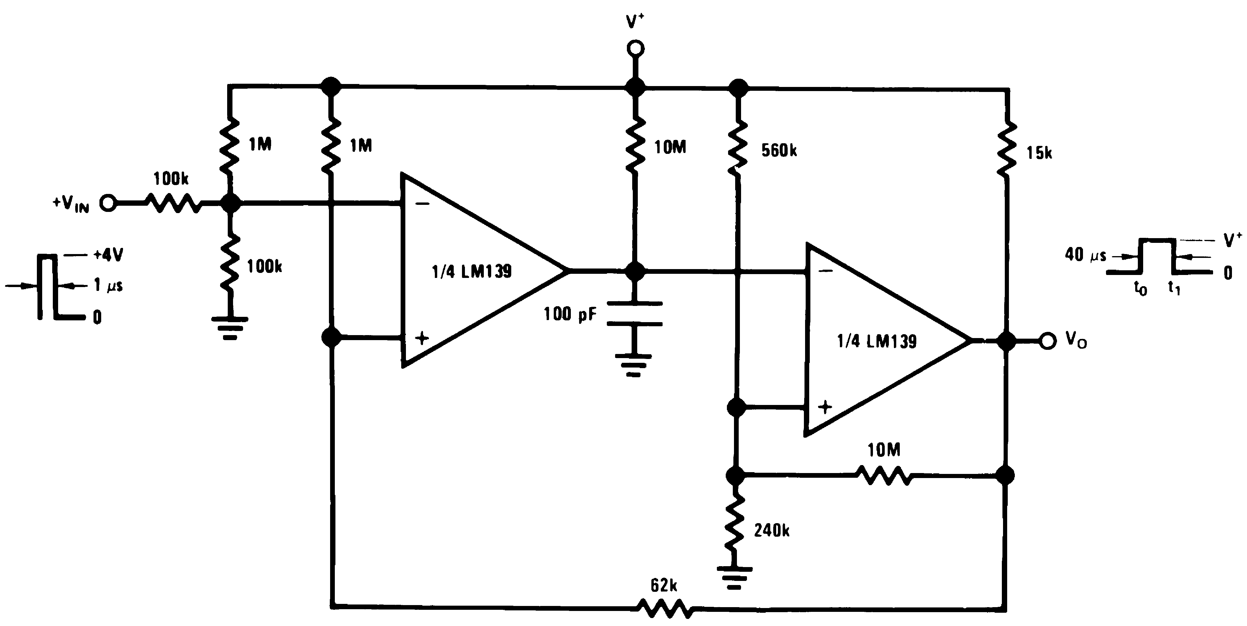
One-Shot Multivibrator With Input Lock Out