SNVS528H October 2007 – January 2016 LM20143 , LM20143-Q1
PRODUCTION DATA.
- 1 Features
- 2 Applications
- 3 Description
- 4 Revision History
- 5 Pin Configuration and Functions
- 6 Specifications
- 7 Detailed Description
-
8 Application and Implementation
- 8.1 Application Information
- 8.2
Typical Applications
- 8.2.1
3.3-V or 5-V Supply Rail Design
- 8.2.1.1 Design Requirements
- 8.2.1.2
Detailed Design Procedure
- 8.2.1.2.1 Duty Cycle Calculation
- 8.2.1.2.2 Inductor Selection (L)
- 8.2.1.2.3 Output Capacitor Selection (COUT)
- 8.2.1.2.4 Input Capacitor Selection (CIN)
- 8.2.1.2.5 Setting the Output Voltage (RFB1, RFB2)
- 8.2.1.2.6 Adjusting the Operating Frequency (RT)
- 8.2.1.2.7 AVIN Filtering Components (CF and RF)
- 8.2.1.2.8 Sub-Regulator Bypass Capacitor (CVCC)
- 8.2.1.2.9 Setting the Start Up Time (CSS)
- 8.2.1.2.10 Loop Compensation (RC1, CC1)
- 8.2.1.3 Application Curves
- 8.2.2 5-V Supply Rail Design
- 8.2.3 3-V Supply Rail Design
- 8.2.1
3.3-V or 5-V Supply Rail Design
- 9 Power Supply Recommendations
- 10Layout
- 11Device and Documentation Support
- 12Mechanical, Packaging, and Orderable Information
Package Options
Mechanical Data (Package|Pins)
- PWP|16
Thermal pad, mechanical data (Package|Pins)
- PWP|16
Orderable Information
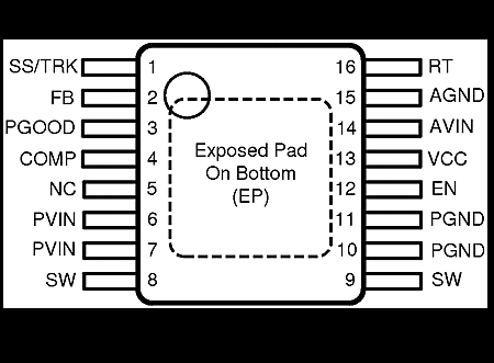
5 Pin Configuration and Functions
PWP Package
16-Pin HTSSOP With Exposed Thermal Pad
Top View

Pin Functions
| PIN | TYPE(1) | DESCRIPTION | |
|---|---|---|---|
| NO. | NAME | ||
| 1 | SS/TRK | I | Soft-Start or Tracking control input. An internal 5-µA current source charges an external capacitor to set the Soft-Start ramp rate. If driven by a external source less than 800 mV, this pin overrides the internal reference that sets the output voltage. If left open, an internal 1ms Soft-Start ramp is activated. |
| 2 | FB | I | Feedback input to the error amplifier from the regulated output. This pin is connected to the inverting input of the internal transconductance error amplifier. An 800-mV reference connected to the non-inverting input of the error amplifier sets the closed loop regulation voltage at the FB pin. |
| 3 | PGOOD | O | Power good output signal. Open drain output indicating the output voltage is regulating within tolerance. is recommend for most applications. |
| 4 | COMP | O | External compensation pin. Connect the compensation network to resistor and capacitor to this pin to compensate the device. |
| 5 | NC | - | This pin has no internal connection. While this pin may be left open, it is strongly recommended that this pin be connected to Ground. |
| 6 | PVIN | P | Input voltage to the power switches inside the device. These pins should be connected together at the device. A low ESR capacitor should be placed near these pins to stabilize the input voltage. |
| 7 | |||
| 8 | SW | P | Switch pin. The PWM output of the internal power switches. |
| 9 | |||
| 10 | PGND | G | Power ground pin for the internal power switches. |
| 11 | |||
| 12 | EN | I | Precision enable input for the device. An external voltage divider can be used to set the device turn-on threshold. If not used the EN pin should be connected to PVIN. |
| 13 | VCC | P | Internal 2.7-V sub-regulator. This pin should be bypassed with a 1-µF ceramic capacitor. |
| 14 | AVIN | P | Analog input supply that generates the internal bias. Must be connected to VIN through a low pass RC filter. |
| 15 | AGND | G | Quiet analog ground for the internal bias circuitry. |
| 16 | RT | I | Frequency adjust pin. Connecting a resistor on this pin to ground will set the oscillator frequency. |
| EP | Exposed Pad | - | Exposed metal thermal pad on the underside of the package with a weak electrical connection to ground. It is recommended to connect this pad to the PC board ground plane copper in order to improve heat dissipation and reduce the package θJA. Do not connect to any potential other than Ground. |
(1) P: Power, I: Input, O: Output, G: Ground