SNVS586O September 2008 – November 2014 LM22673 , LM22673-Q1
PRODUCTION DATA.
- 1 Features
- 2 Applications
- 3 Description
- 4 Revision History
- 5 Pin Configuration and Functions
- 6 Specifications
- 7 Detailed Description
- 8 Applications and Implementation
- 9 Power Supply Recommendations
- 10Layout
- 11Device and Documentation Support
- 12Mechanical, Packaging, and Orderable Information
Package Options
Mechanical Data (Package|Pins)
Thermal pad, mechanical data (Package|Pins)
- DDA|8
Orderable Information
6 Specifications
6.1 Absolute Maximum Ratings
over operating free-air temperature range (unless otherwise noted)| MIN | MAX | UNIT | ||
|---|---|---|---|---|
| VIN to GND | 43 | V | ||
| SS, IADJ Pin Voltage | –0.5 | 7 | V | |
| SW to GND(1) | –5 | VIN | V | |
| Boot Pin Voltage | VSW + 7 | V | ||
| FB Pin Voltage | –0.5 | 7 | V | |
| Power Dissipation | Internally Limited | |||
| Junction Temperature | 150 | °C | ||
| For soldering specifications, refer to Application Report Absolute Maximum Ratings for Soldering (SNOA549). | ||||
6.2 Handling Ratings
| MIN | MAX | UNIT | |||
|---|---|---|---|---|---|
| Tstg | Storage temperature range | –65 | 150 | °C | |
| V(ESD) | Electrostatic discharge | Human body model (HBM), per ANSI/ESDA/JEDEC JS-001, all pins(1) | –2 | 2 | V |
(1) JEDEC document JEP155 states that 500-V HBM allows safe manufacturing with a standard ESD control process.
6.3 Handling Ratings: LM22673-Q1
| MIN | MAX | UNIT | ||||
|---|---|---|---|---|---|---|
| Tstg | Storage temperature range | –65 | 150 | °C | ||
| V(ESD) | Electrostatic discharge | Human body model (HBM), per AEC Q100-002(1) | –2 | 2 | kV | |
(1) AEC Q100-002 indicates HBM stressing is done in accordance with the ANSI/ESDA/JEDEC JS-001 specification.
6.4 Recommended Operating Conditions
| MIN | MAX | UNIT | ||
|---|---|---|---|---|
| VIN | Supply Voltage | 4.5 | 42 | V |
| Junction Temperature | –40 | 125 | °C | |
6.5 Thermal Information
| THERMAL METRIC(1) | LM22673 | UNIT | ||
|---|---|---|---|---|
| DDA | NDR | |||
| 8 PINS | 7 PINS | |||
| RθJA | Junction-to-ambient thermal resistance | 60 | 22 | °C/W |
(1) For more information about traditional and new thermal metrics, see the IC Package Thermal Metrics application report (SPRA953).
6.6 Electrical Characteristics
Typical values represent the most likely parametric norm at TA = TJ = 25°C, and are provided for reference purposes only. Unless otherwise specified: VIN = 12 V.| PARAMETER | TEST CONDITIONS | MIN(3) | TYP(2) | MAX(3) | UNIT | |
|---|---|---|---|---|---|---|
| LM22673-5.0 | ||||||
| VFB | Feedback Voltage | VIN = 8 V to 42 V | 4.925 | 5.0 | 5.075 | V |
| VIN = 8 V to 42 V, –40°C ≤ TJ ≤ 125°C | 4.9 | 5.1 | ||||
| LM22673-ADJ | ||||||
| VFB | Feedback Voltage | VIN = 4.7 V to 42 V | 1.266 | 1.285 | 1.304 | V |
| VIN = 4.7 V to 42 V, –40°C ≤ TJ ≤ 125°C | 1.259 | 1.311 | ||||
| ALL OUTPUT VOLTAGE VERSIONS | ||||||
| IQ | Quiescent Current | VFB = 5 V | 3.4 | mA | ||
| VFB = 5 V, –40°C ≤ TJ ≤ 125°C | 6 | |||||
| VADJ | Current Limit Adjust Voltage | 0.8 | V | |||
| –40°C ≤ TJ ≤ 125°C | 0.65 | 0.9 | ||||
| ICL | Current Limit | 3.4 | 4.2 | 5.3 | A | |
| –40°C ≤ TJ ≤ 125°C | 3.35 | 5.5 | ||||
| RDS(ON) | Switch On-Resistance | PFM Package | 0.12 | 0.16 | Ω | |
| PFM Package, –40°C ≤ TJ ≤ 125°C | 0.22 | |||||
| SO PowerPAD Package | 0.10 | 0.16 | ||||
| SO PowerPAD Package, –40°C ≤ TJ ≤ 125°C | 0.20 | |||||
| fO | Oscillator Frequency | 500 | kHz | |||
| –40°C ≤ TJ ≤ 125°C | 400 | 600 | ||||
| TOFFMIN | Minimum Off-time | 200 | ns | |||
| –40°C ≤ TJ ≤ 125°C | 100 | 300 | ||||
| TONMIN | Minimum On-time | 100 | ns | |||
| IBIAS | Feedback Bias Current | VFB = 1.3 V (ADJ Version Only) | 230 | nA | ||
| ISS | Soft-start Current | EN Input = 0 V | 50 | µA | ||
| EN Input = 0 V, –40°C ≤ TJ ≤ 125°C | 30 | 70 | ||||
| TSD | Thermal Shutdown Threshold | 150 | °C | |||
(1) The absolute maximum specification of the ‘SW to GND’ applies to dc voltage. An extended negative voltage limit of –10 V applies to a pulse of up to 50 ns.
(2) Typical values represent most likely parametric norms at the conditions specified and are not ensured.
(3) MIN and MAX limits are 100% production tested at 25°C. Limits over the operating temperature range are ensured through correlation using Statistical Quality Control (SQC) methods. Limits are used to calculate TI's Average Outgoing Quality Level (AOQL).
6.7 Typical Characteristics
Vin = 12 V, TJ = 25°C (unless otherwise specified)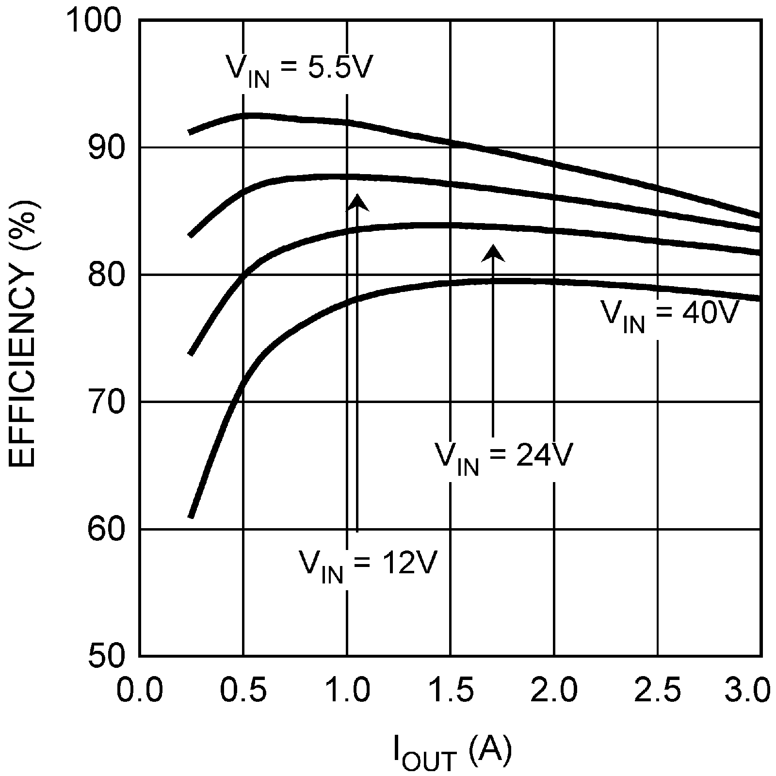 Figure 1. Efficiency vs IOUT and VIN
VOUT = 3.3 V
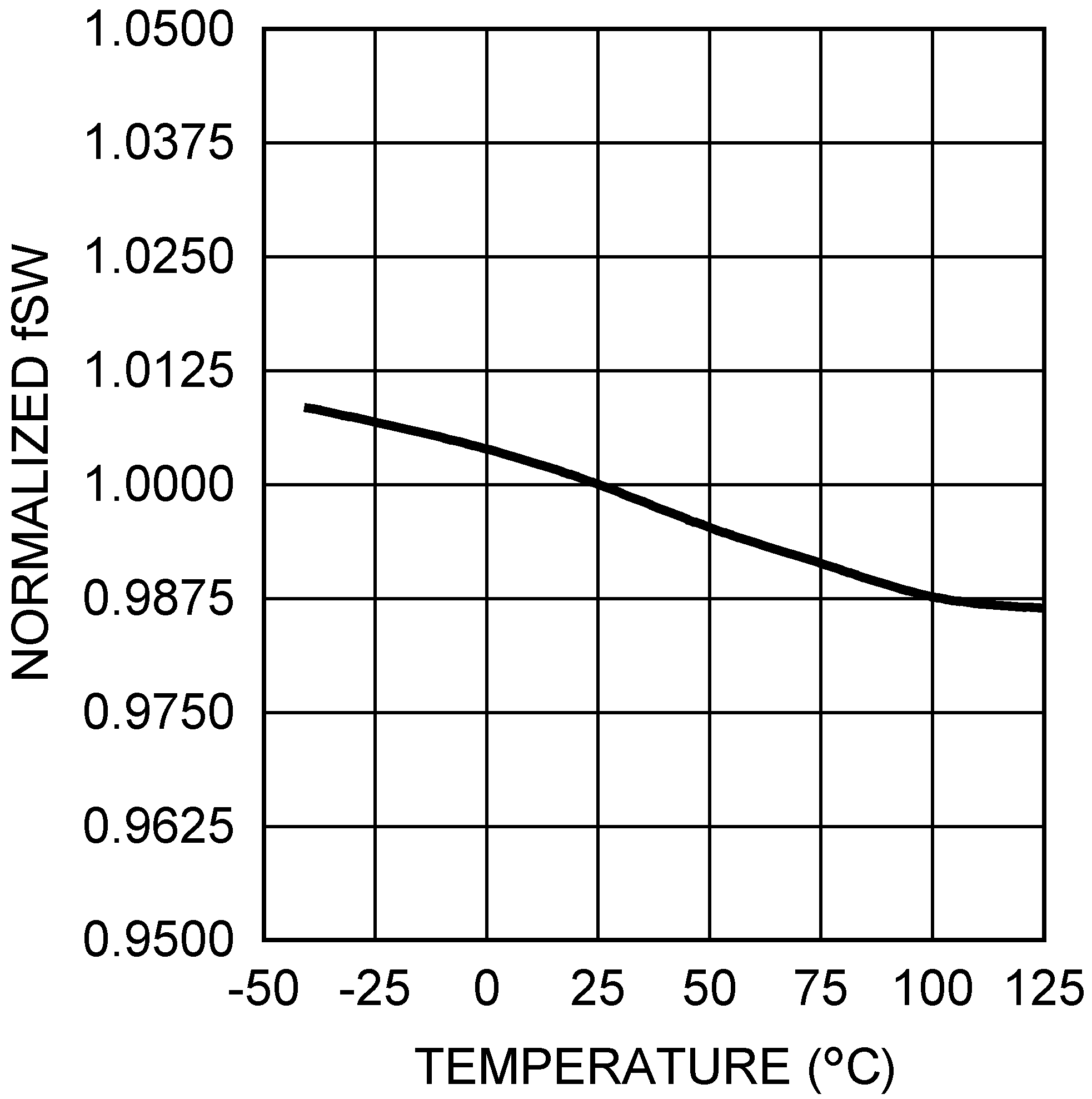 Figure 3. Normalized Switching Frequency vs Temperature
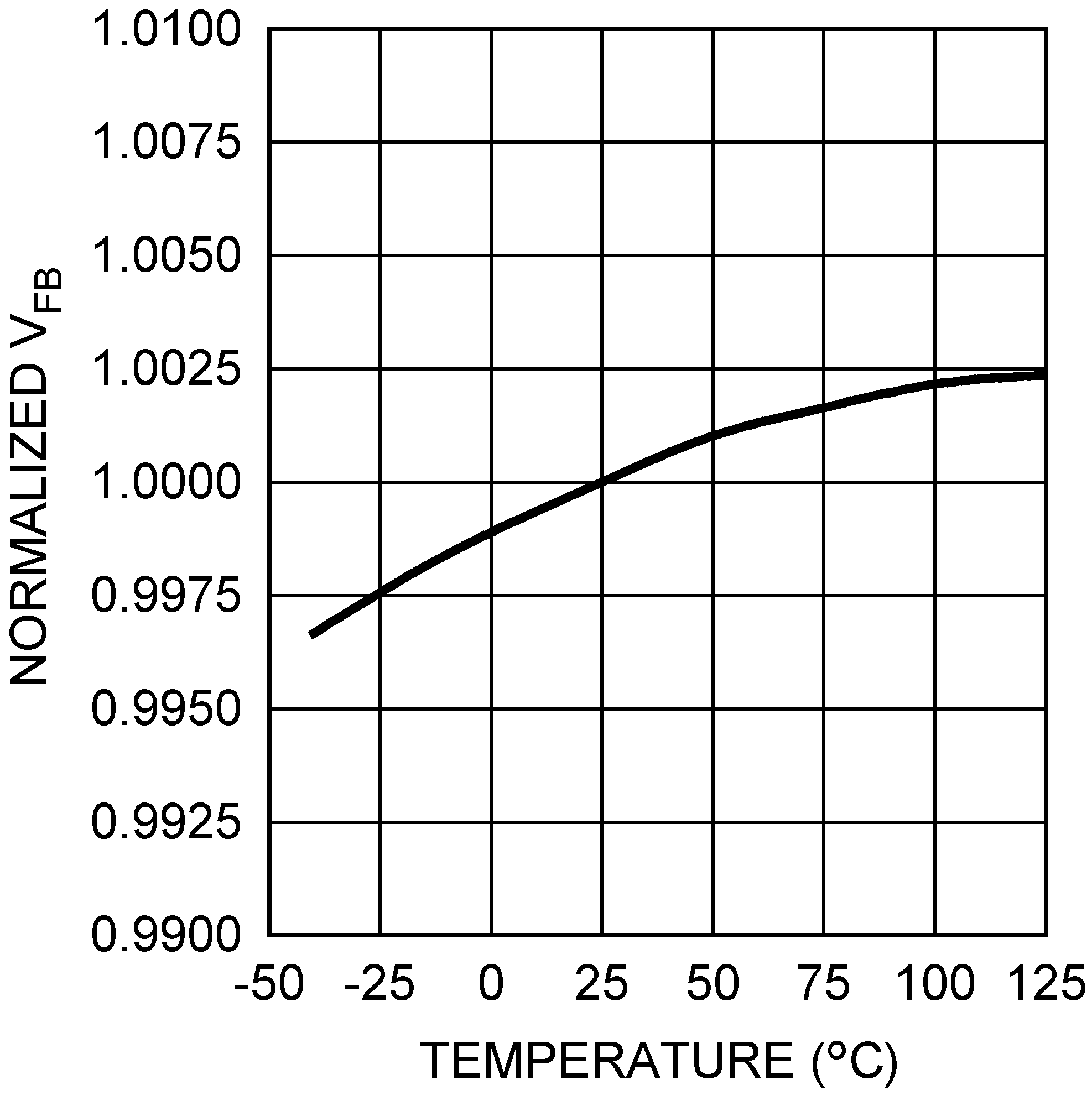 Figure 5. Normalized Feedback Voltage vs Temperature
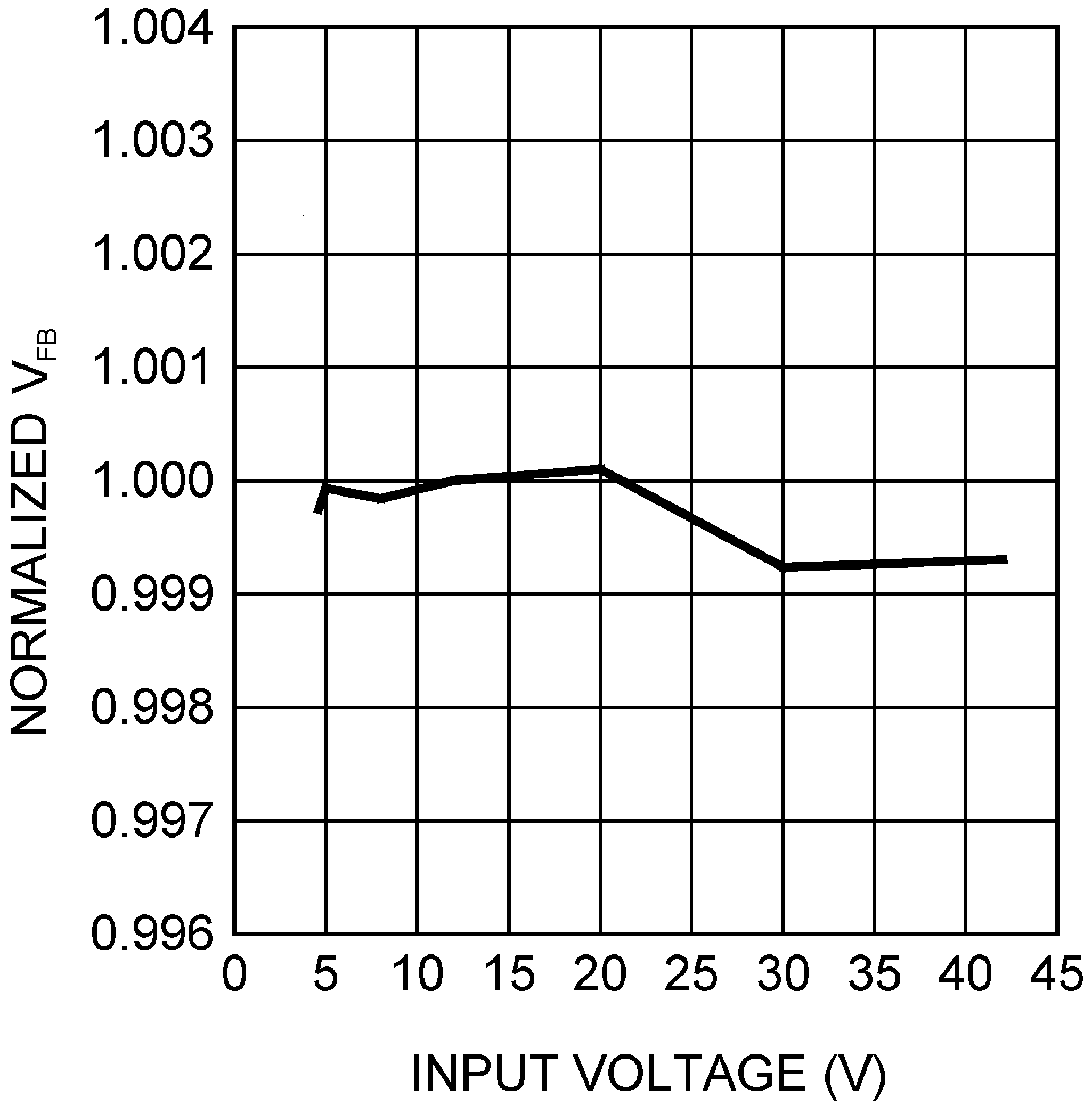 Figure 7. Normalized Feedback Voltage vs Input Voltage
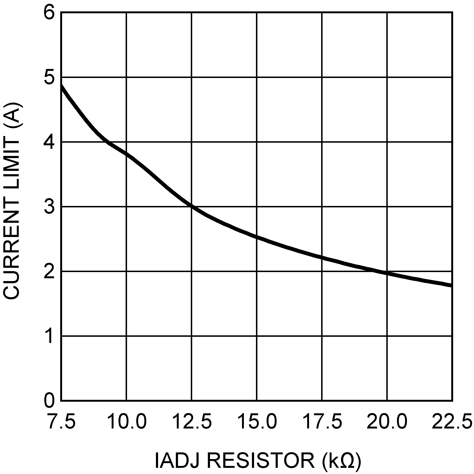 Figure 9. Current Limit vs IADJ Resistor
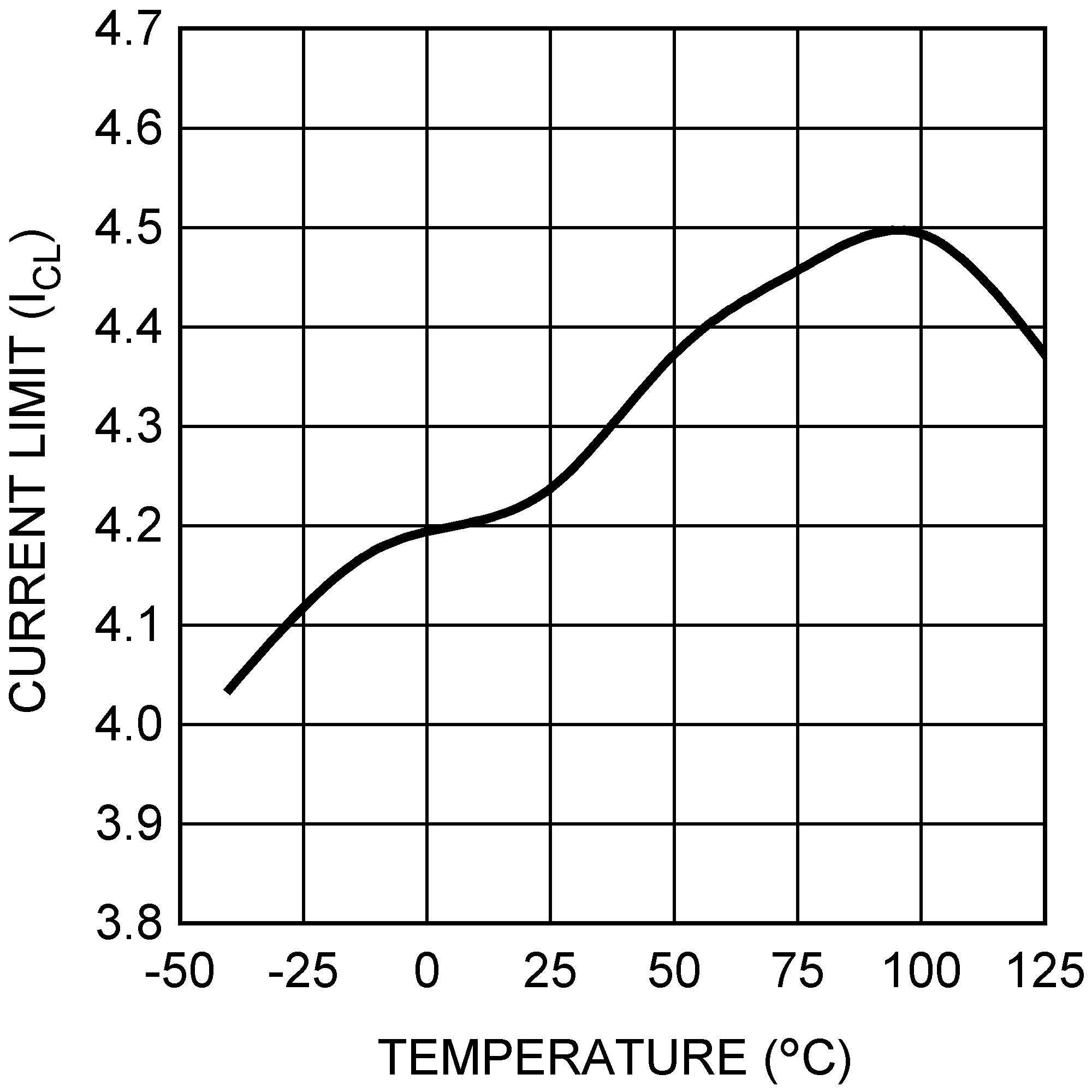 Figure 2. Current Limit vs Temperature
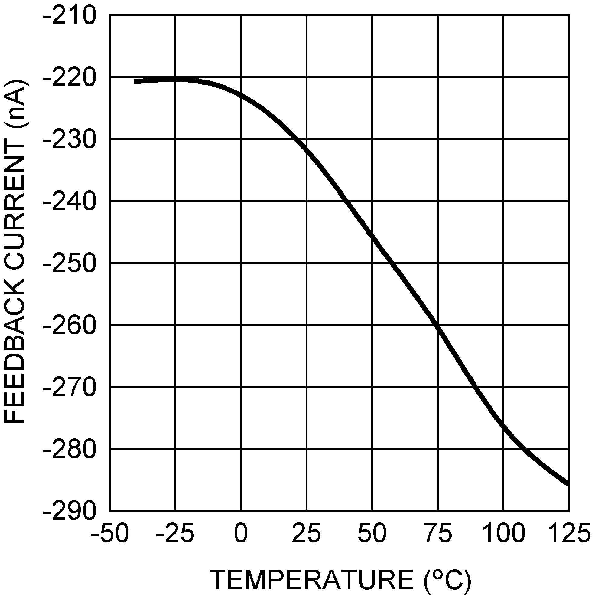 Figure 4. Feedback Bias Current vs Temperature
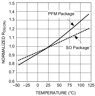 Figure 6. Normalized RDS(ON) vs Temperature
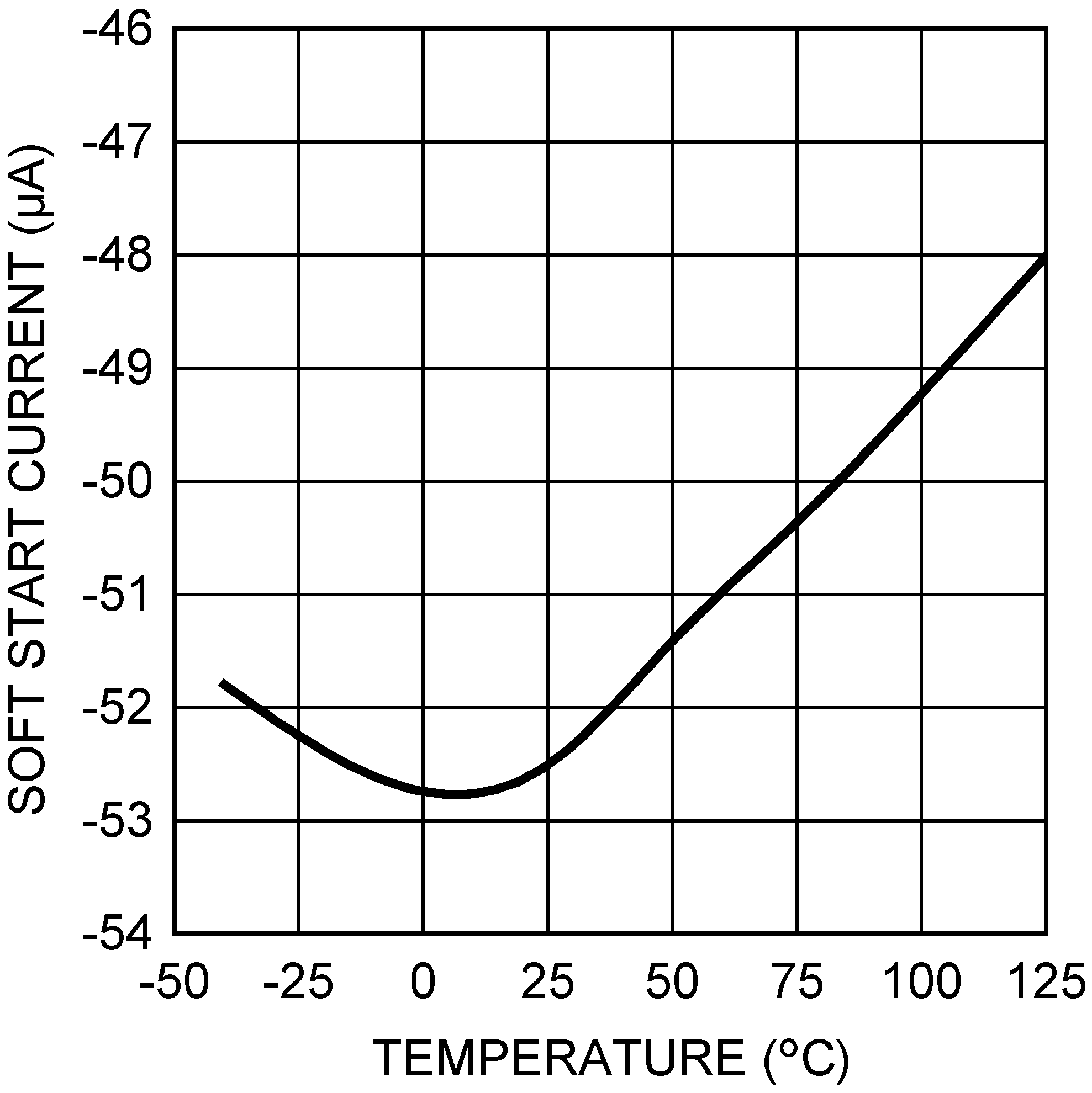 Figure 8. Soft-Start Current vs Temperature