SNVS587L September 2008 – November 2014 LM22676 , LM22676-Q1
PRODUCTION DATA.
- 1 Features
- 2 Applications
- 3 Description
- 4 Revision History
- 5 Pin Configuration and Functions
- 6 Specifications
- 7 Detailed Description
- 8 Application and Implementation
- 9 Power Supply Recommendations
- 10Layout
- 11Device and Documentation Support
- 12Mechanical, Packaging, and Orderable Information
Package Options
Mechanical Data (Package|Pins)
Thermal pad, mechanical data (Package|Pins)
- DDA|8
Orderable Information
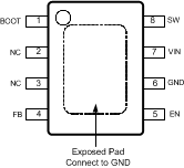
5 Pin Configuration and Functions
SO PowerPAD Package
8-Pin
Top View
PFM Package
8-Pin
Top View
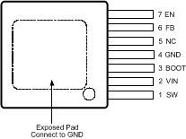
Pin Functions
| PIN | TYPE | DESCRIPTION | APPLICATION INFORMATION | ||
|---|---|---|---|---|---|
| NAME | SO PowerPAD |
PFM | |||
| BOOT | 1 | 3 | I | Bootstrap input | Provides the gate voltage for the high side N-FET. |
| NC | 2, 3 | 5 | — | Not Connected | Pins are not electrically connected inside the chip. Pins do function as thermal conductor. |
| FB | 4 | 6 | I | Feedback pin | Feedback input to regulator. |
| EN | 5 | 7 | I | Enable input | Used to control regulator start-up and shutdown. See Precision Enable and UVLO section of data sheet. |
| GND | 6 | 4 | — | Ground input to regulator; system common |
System ground pin. |
| VIN | 7 | 2 | I | Input Voltage | Input supply to regulator |
| SW | 8 | 1 | O | Switch pin | Switching output of regulator |
| EP | EP | EP | — | Exposed Pad | Connect to ground. Provides thermal connection to PCB. See Thermal Considerations. |