SNVS581M February 2013 – October 2020 LM22679 , LM22679-Q1
PRODUCTION DATA
- 1 Features
- 2 Applications
- 3 Description
- 4 Revision History
- 5 Pin Configuration and Functions
- 6 Specifications
- 7 Detailed Description
- 8 Application and Implementation
- 9 Power Supply Recommendations
- 10Layout
- 11Device and Documentation Support
Package Options
Mechanical Data (Package|Pins)
- NDR|7
Thermal pad, mechanical data (Package|Pins)
Orderable Information
7.3.4 Internal Compensation
The LM22679 device has internal loop compensation designed to provide a stable regulator over a wide range of external power stage components. The internal compensation of the -ADJ option is optimized for output voltages below 5 V. If an output voltage of 5 V or greater is needed, the -5.0 option with an external resistor divider can be used.
Ensuring stability of a design with a specific power stage (inductor and output capacitor) can be tricky. The LM22679 stability can be verified using the WEBENCH Designer online circuit simulation tool. A quick start spreadsheet can also be downloaded from the online product folder.
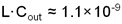
The complete transfer function for the regulator loop is found by combining the compensation and power stage transfer functions. The LM22679 has internal type III loop compensation, as detailed in Internal Loop Compensation section. This is the approximate "straight line" function from the FB pin to the input of the PWM modulator. The power stage transfer function consists of a dc gain and a second order pole created by the inductor and output capacitor or capacitors. Due to the input voltage feedforward employed in the LM22679, the power stage dc gain is fixed at 20 dB. The second order pole is characterized by its resonant frequency and its quality factor (Q). For a first pass design, the product of inductance and output capacitance should conform to Equation 2.
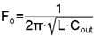
Alternatively, this pole should be placed between 1.5 kHz and 15 kHz and is given by Equation 3.
The Q factor depends on the parasitic resistance of the power stage components and is not typically in the control of the designer. Of course, loop compensation is only one consideration when selecting power stage components (see Section 8 for more details).
 Figure 7-1 Compensator Gain
In general, hand calculations or simulations can only aid in selecting good power stage components. Good design practice dictates that load and line transient testing should be done to verify the stability of the application. Also, Bode plot measurements should be made to determine stability margins. The AN-1889 How to Measure the Loop Transfer Function of Power Supplies application report (SNVA364) shows how to perform a loop transfer function measurement with only an oscilloscope and function generator.