SNVS617H April   2009  – November 2014 LM25011 , LM25011-Q1

PRODUCTION DATA.  

  1. Features
  2. Applications
  3. Description
    1.     Typical Application
  4. Revision History
  5. Pin Configuration and Functions
    1.     Pin Functions
  6. Specifications
    1. 6.1 Absolute Maximum Ratings
    2. 6.2 Handling Ratings: LM25011
    3. 6.3 Handling Ratings: LM25011-Q1
    4. 6.4 Recommended Operating Conditions
    5. 6.5 Thermal Information
    6. 6.6 Electrical Characteristics
    7. 6.7 Typical Characteristics
  7. Detailed Description
    1. 7.1 Overview
    2. 7.2 Functional Block Diagram
    3. 7.3 Feature Description
      1. 7.3.1 Control Circuit Overview
      2. 7.3.2 On-Time Timer
      3. 7.3.3 Current Limit
      4. 7.3.4 Ripple Requirements
      5. 7.3.5 N-Channel Buck Switch and Driver
      6. 7.3.6 Soft-Start
      7. 7.3.7 Power Good Output (PGD)
      8. 7.3.8 Thermal Shutdown
    4. 7.4 Device Functional Modes
      1. 7.4.1 Shutdown Function
  8. Application and Implementation
    1. 8.1 Application Information
    2. 8.2 Typical Application
      1. 8.2.1 LM25011 Example Circuit
        1. 8.2.1.1 Design Requirements
        2. 8.2.1.2 Detailed Design Procedure
          1. 8.2.1.2.1 Custom Design with WEBENCH Tools
          2. 8.2.1.2.2 External Components
        3. 8.2.1.3 Application Curves
      2. 8.2.2 Output Ripple Control
        1. 8.2.2.1 Option A: Lowest Cost Configuration
        2. 8.2.2.2 Option B: Intermediate VOUT Ripple Configuration
        3. 8.2.2.3 Option C: Minimum VOUT Ripple Configuration
  9. Power Supply Recommendations
  10. 10Layout
    1. 10.1 Layout Guidelines
    2. 10.2 Layout Example
    3. 10.3 Power Dissipation
  11. 11Device and Documentation Support
    1. 11.1 Custom Design with WEBENCH Tools
    2. 11.2 Receiving Notification of Documentation Updates
    3. 11.3 Related Links
    4. 11.4 Trademarks
    5. 11.5 Electrostatic Discharge Caution
    6. 11.6 Glossary
  12. 12Mechanical, Packaging, and Orderable Information

Package Options

Mechanical Data (Package|Pins)
Thermal pad, mechanical data (Package|Pins)
Orderable Information

Typical Characteristics

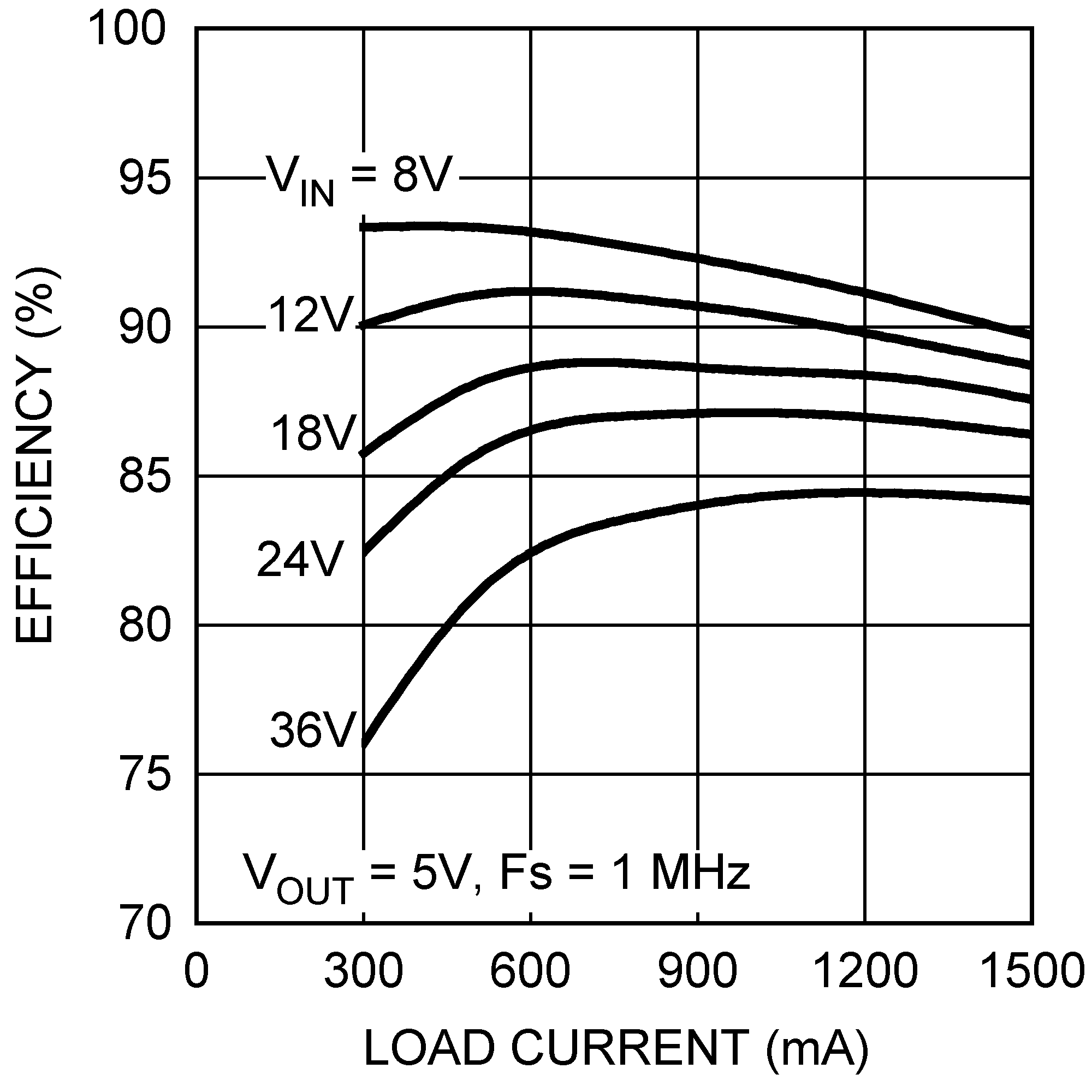
LM25011 LM25011-Q1 LM25011A LM25011A-Q1 30094603.pngFigure 1. Efficiency (Circuit of Figure 19)
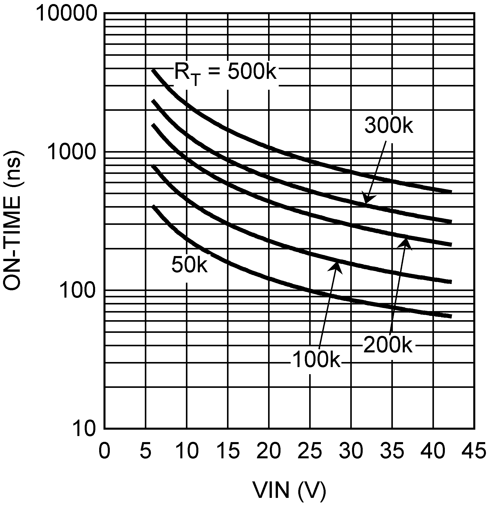
LM25011 LM25011-Q1 LM25011A LM25011A-Q1 30094605.pngFigure 3. On-Time vs VIN and RT
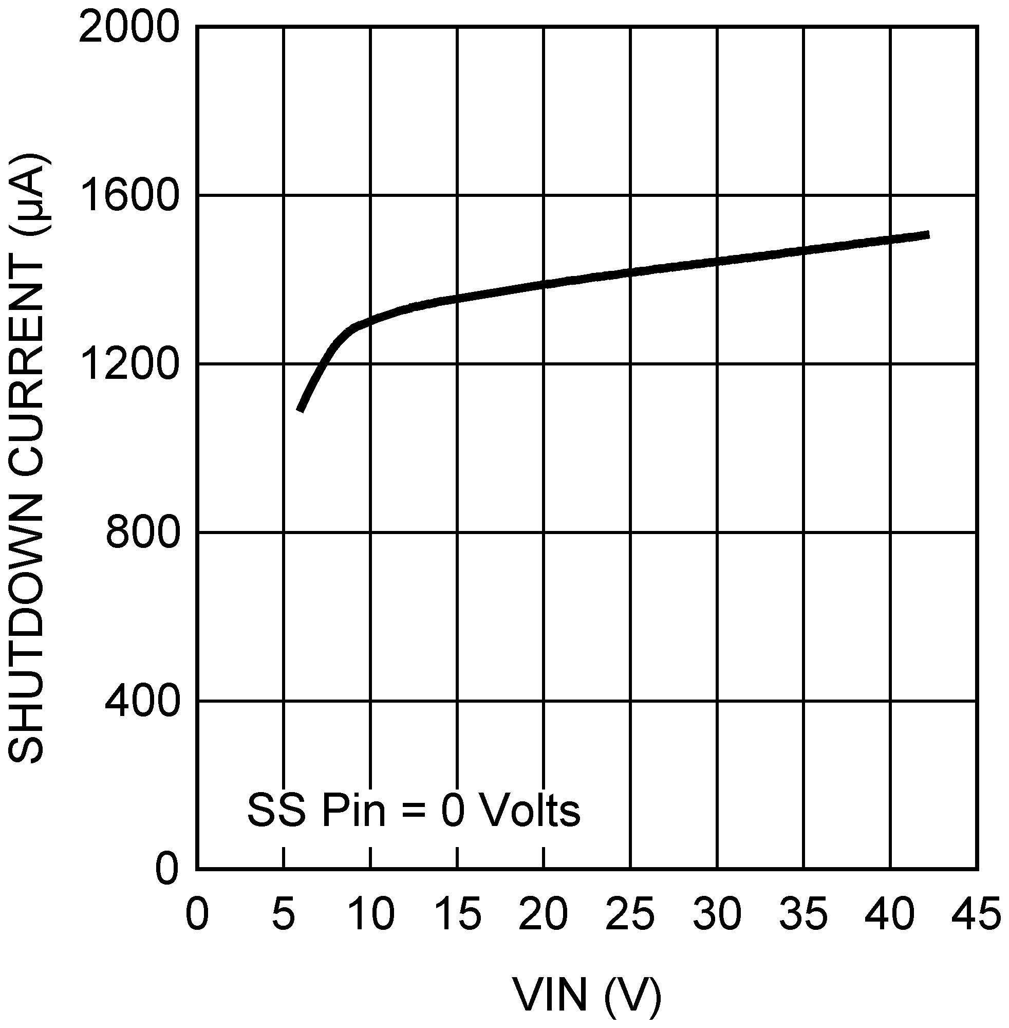
LM25011 LM25011-Q1 LM25011A LM25011A-Q1 30094607.pngFigure 5. Shutdown Current into VIN
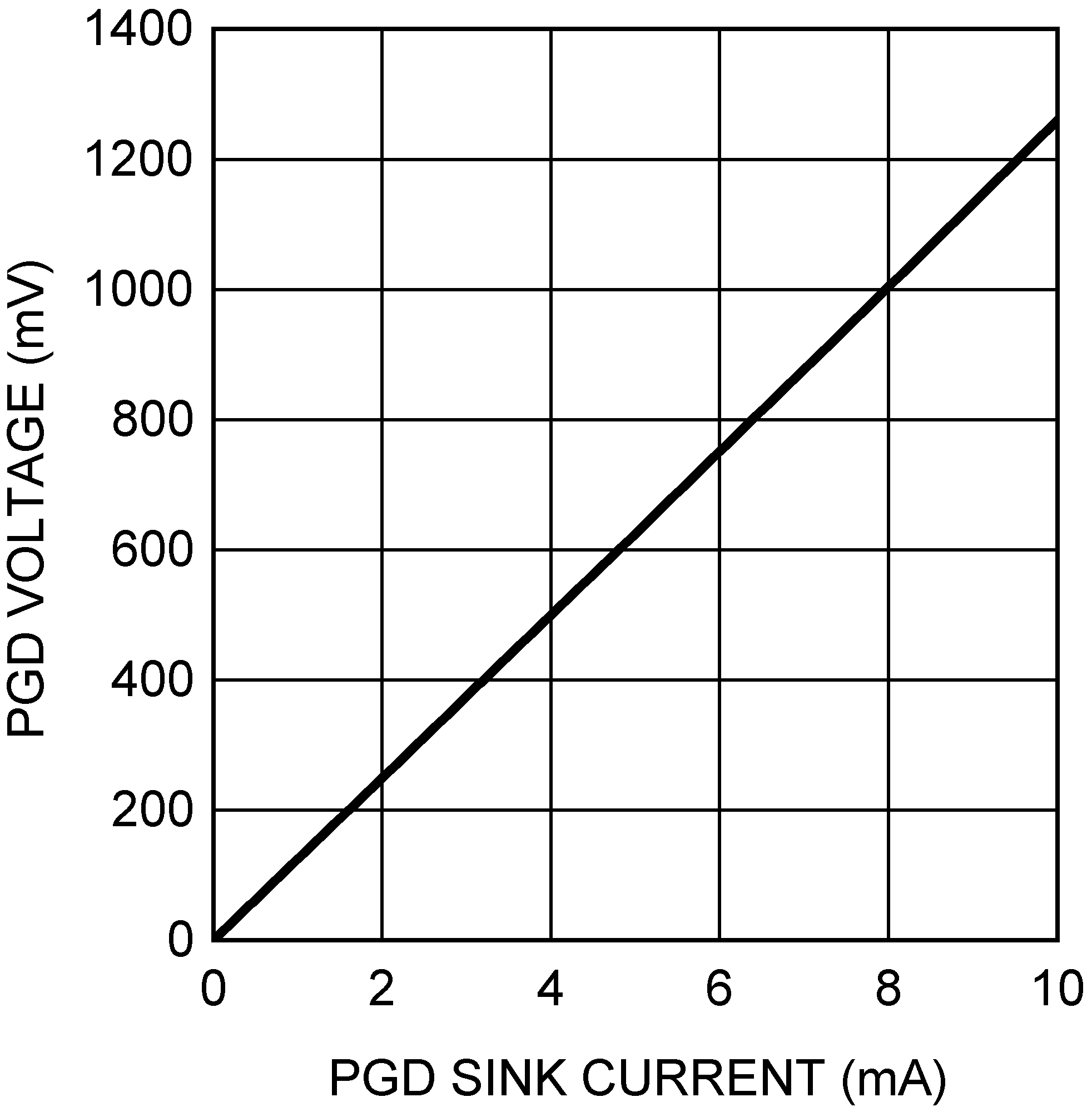
LM25011 LM25011-Q1 LM25011A LM25011A-Q1 30094609.pngFigure 7. PGD Low Voltage vs Sink Current
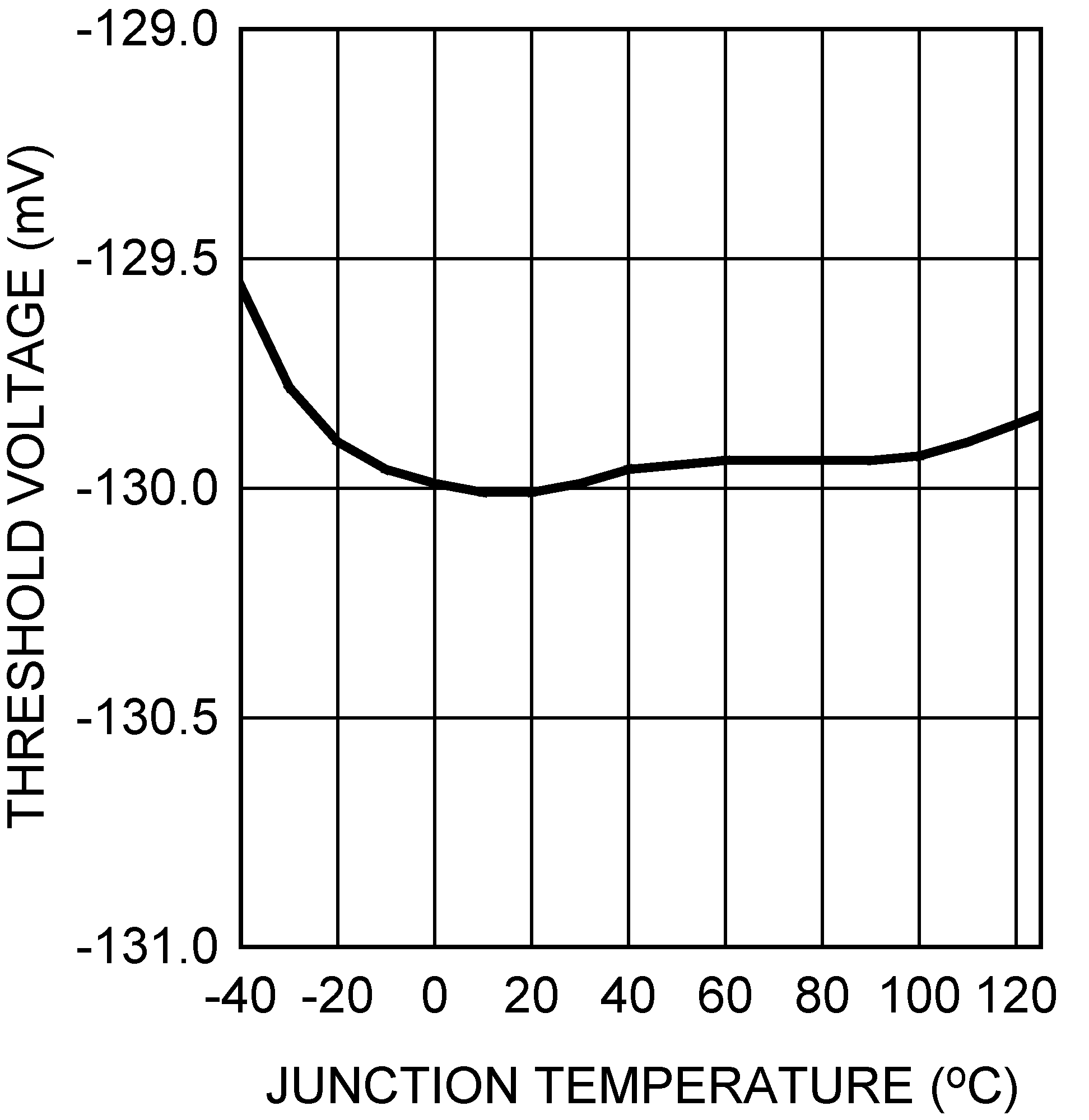
LM25011 LM25011-Q1 LM25011A LM25011A-Q1 30094611.pngFigure 9. Current Limit Threshold vs Temperature
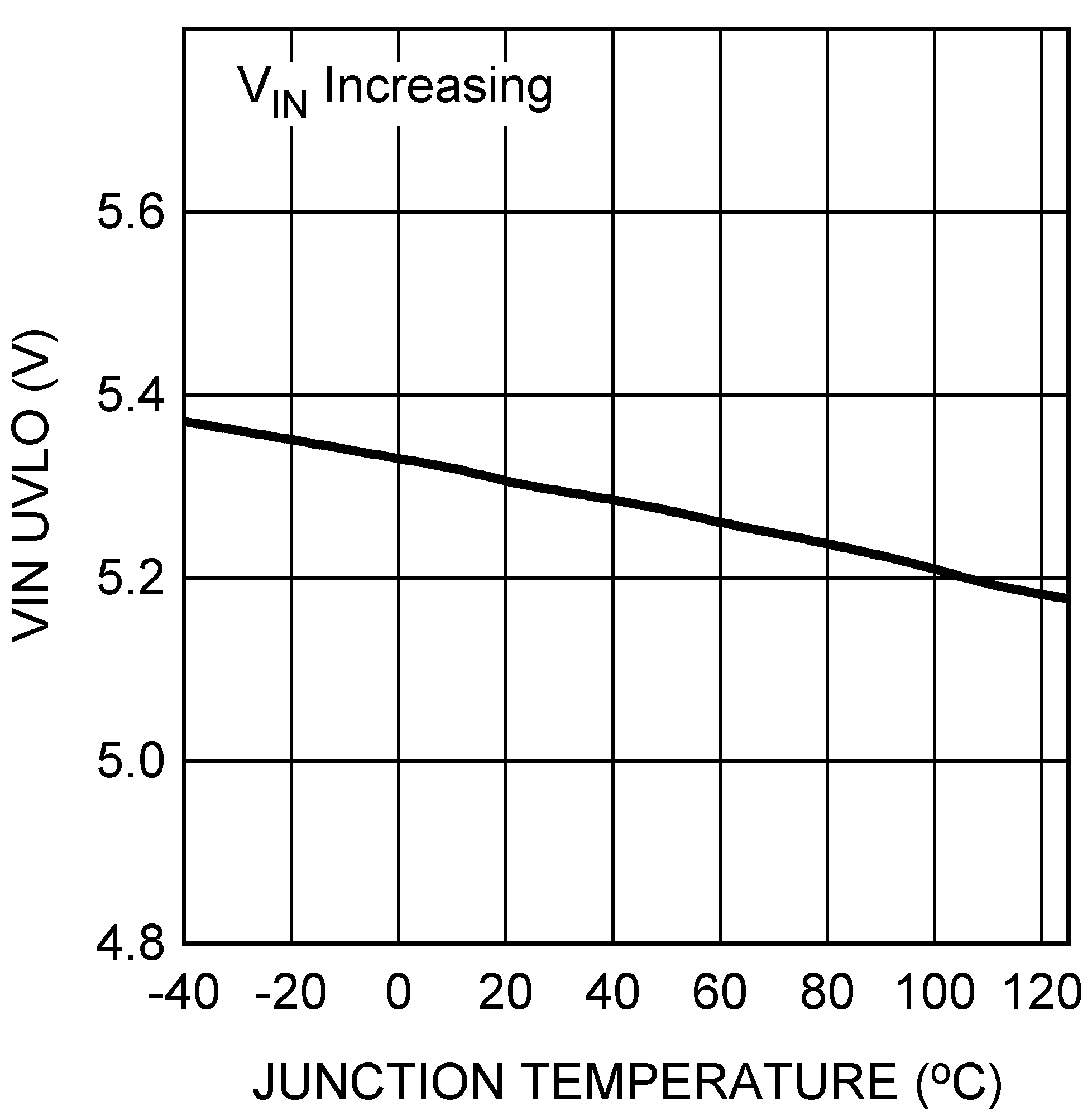
LM25011 LM25011-Q1 LM25011A LM25011A-Q1 30094613.pngFigure 11. VIN UVLO vs Temperature
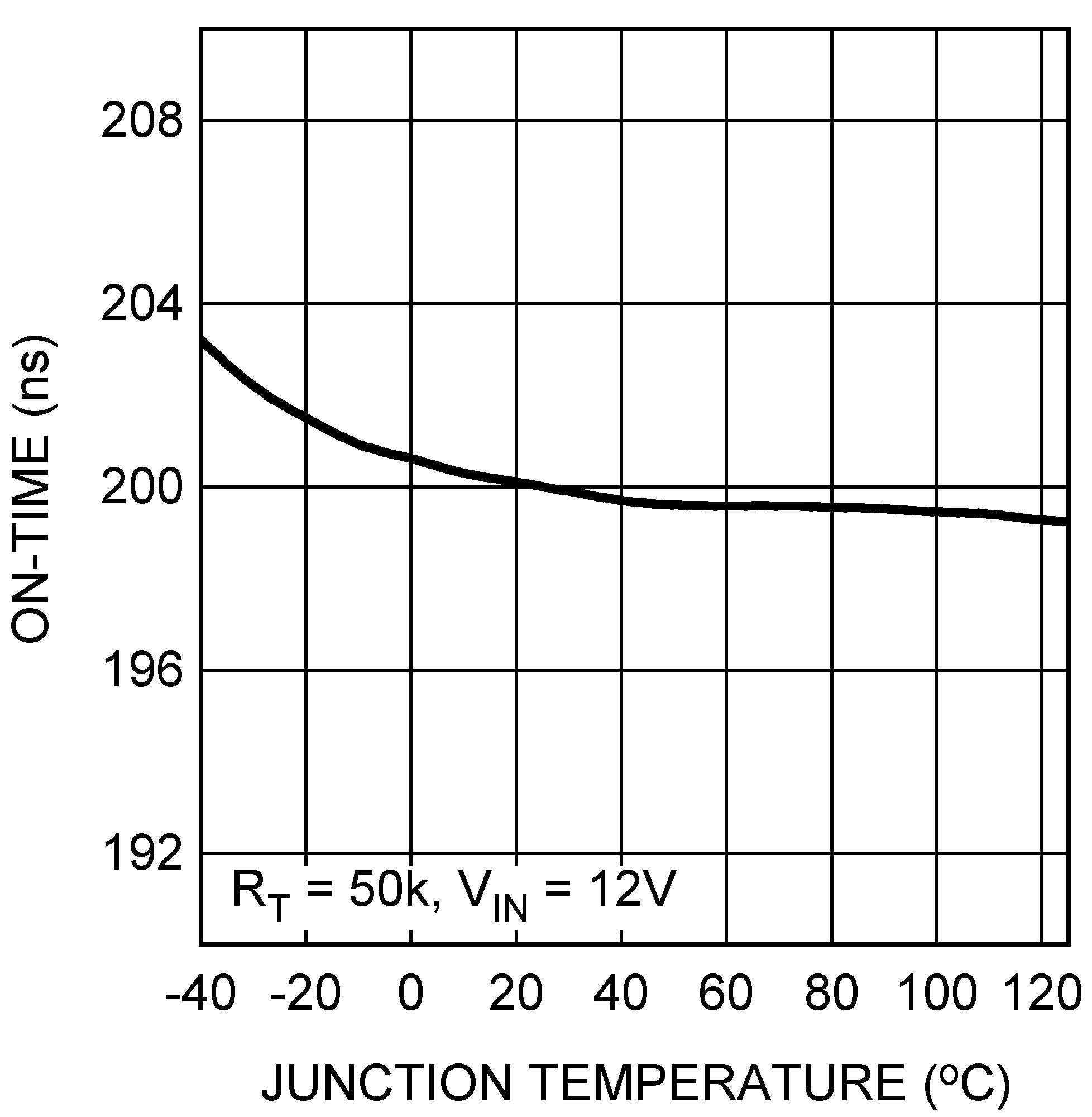
LM25011 LM25011-Q1 LM25011A LM25011A-Q1 30094615.pngFigure 13. On-Time vs Temperature
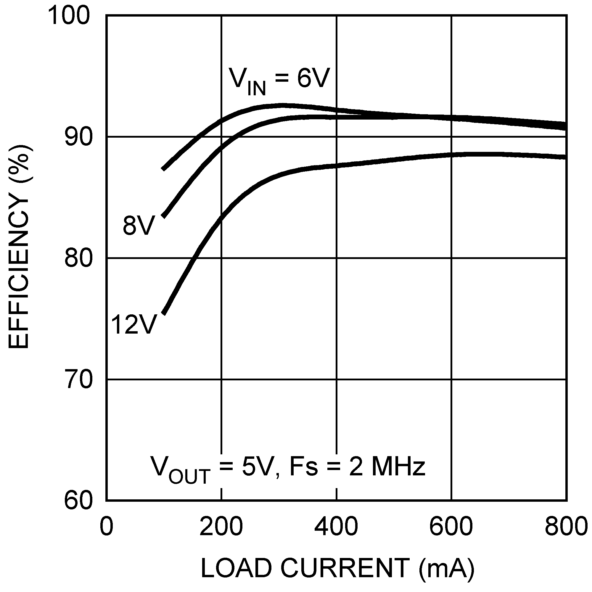
LM25011 LM25011-Q1 LM25011A LM25011A-Q1 30094604.pngFigure 2. Efficiency at 2 MHz
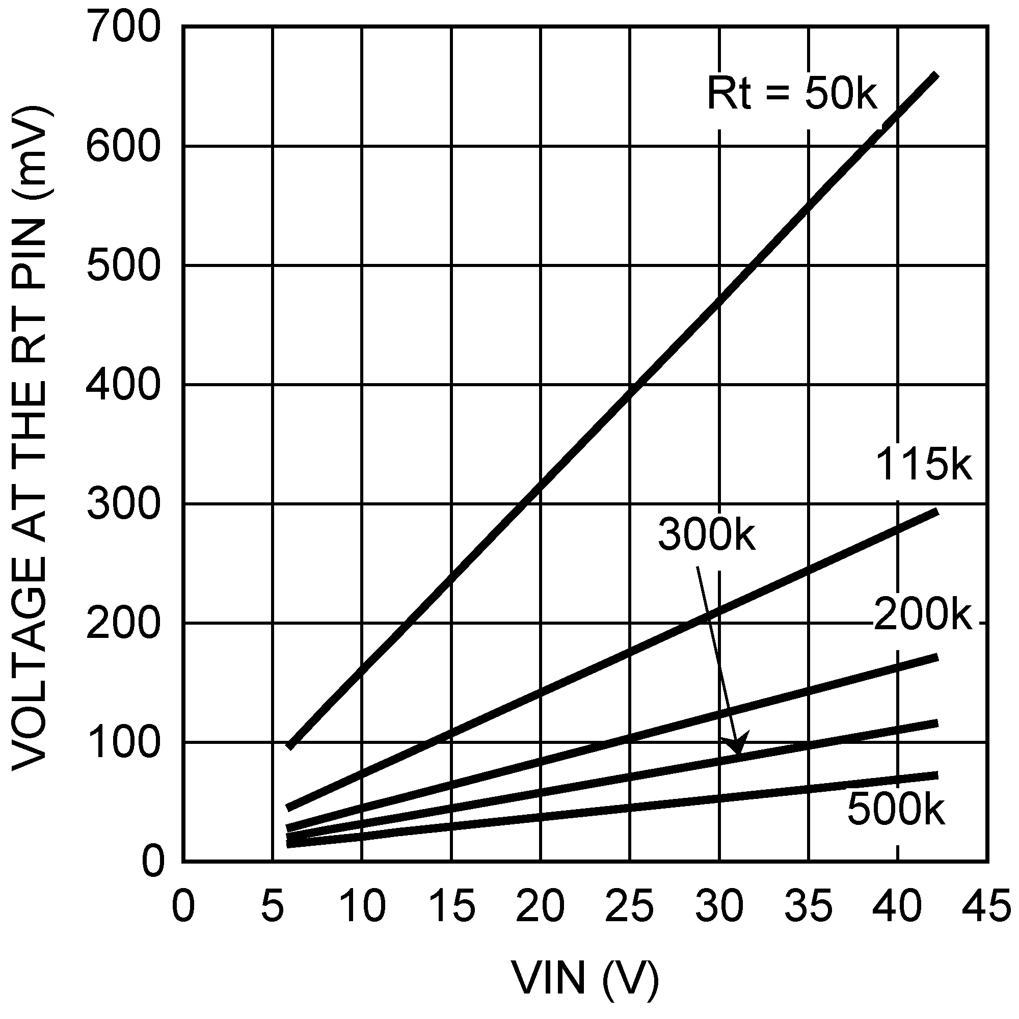
LM25011 LM25011-Q1 LM25011A LM25011A-Q1 30094606.pngFigure 4. Voltage at the RT Pin
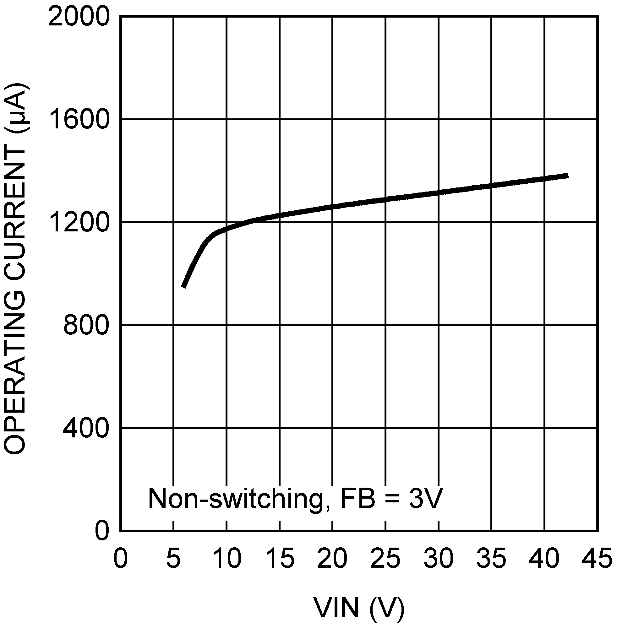
LM25011 LM25011-Q1 LM25011A LM25011A-Q1 30094608.pngFigure 6. Operating Current into VIN
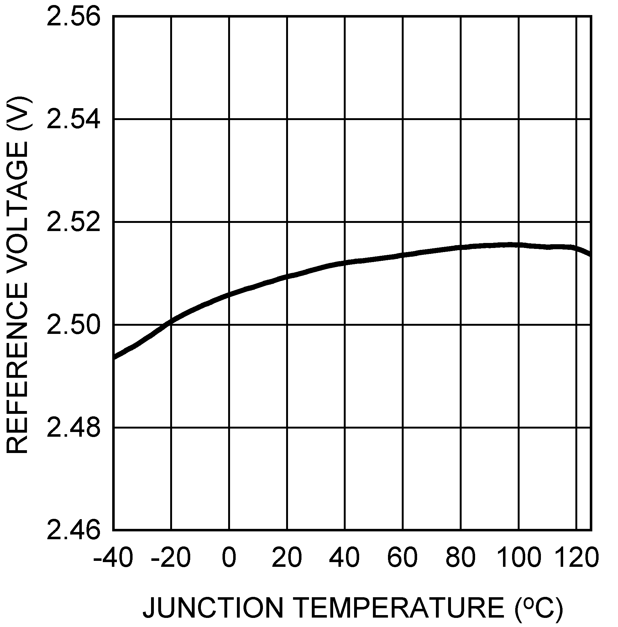
LM25011 LM25011-Q1 LM25011A LM25011A-Q1 30094610.pngFigure 8. Reference Voltage vs Temperature
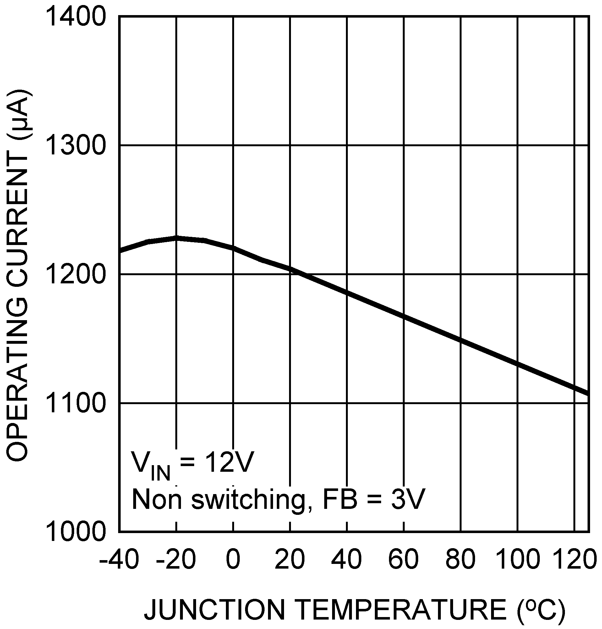
LM25011 LM25011-Q1 LM25011A LM25011A-Q1 30094612.pngFigure 10. Operating Current vs Temperature
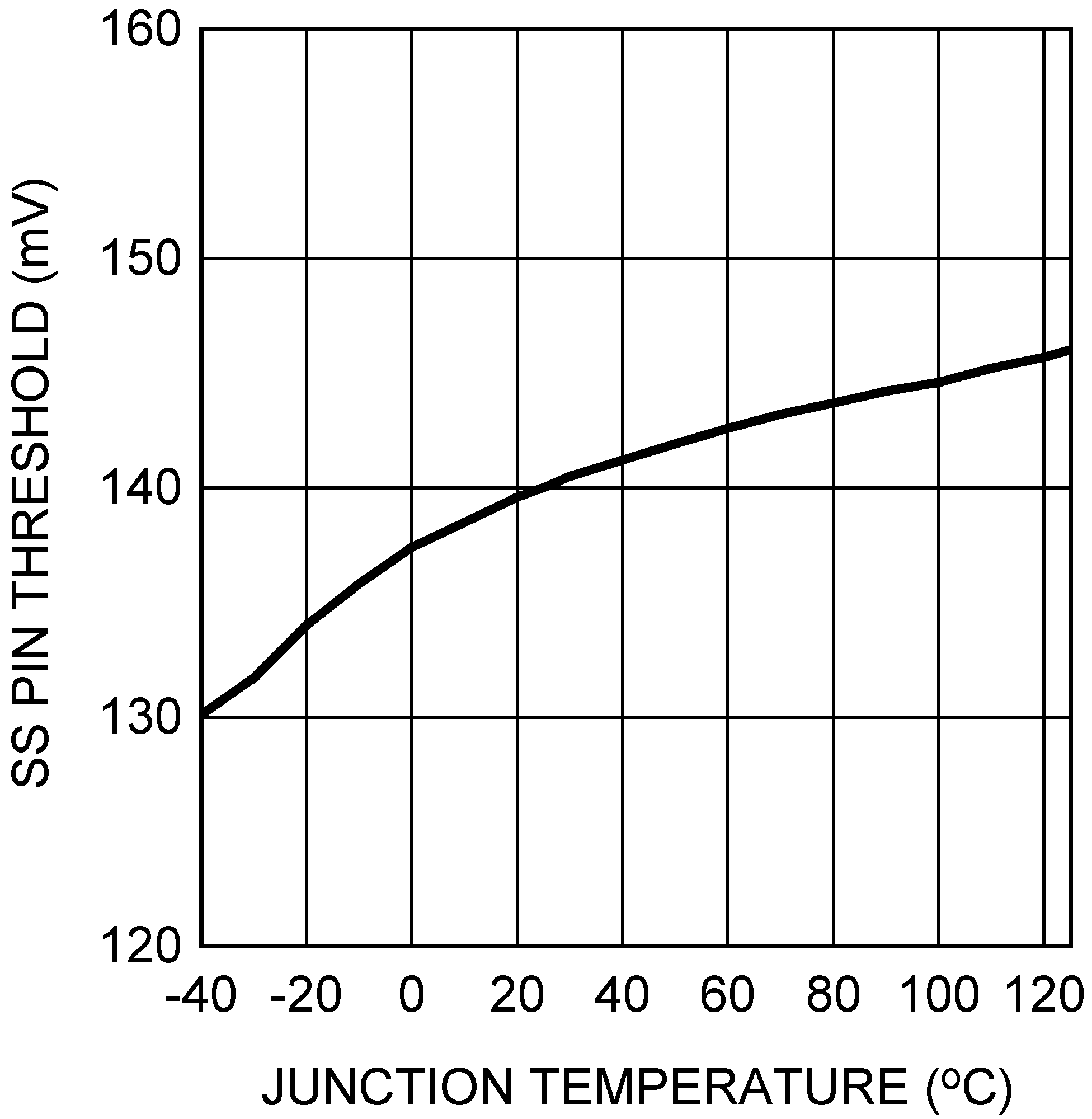
LM25011 LM25011-Q1 LM25011A LM25011A-Q1 30094614.pngFigure 12. SS Pin Shutdown Threshold vs Temperature
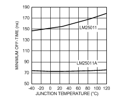
LM25011 LM25011-Q1 LM25011A LM25011A-Q1 30094651.gifFigure 14. Minimum Off-Time vs Temperature