SNVS609K December 2008 – June 2022 LM25088 , LM25088-Q1
PRODUCTION DATA
- 1 Features
- 2 Applications
- 3 Description
- 4 Revision History
- 5 Pin Configuration and Functions
- 6 Specifications
-
7 Detailed Description
- 7.1 Overview
- 7.2 Functional Block Diagram
- 7.3
Feature Description
- 7.3.1 High Voltage Low-Dropout Regulator
- 7.3.2 Line Undervoltage Detector
- 7.3.3 Oscillator and Sync Capability
- 7.3.4 Error Amplifier and PWM Comparator
- 7.3.5 Ramp Generator
- 7.3.6 Dropout Voltage Reduction
- 7.3.7 Frequency Dithering (LM25088-1 Only)
- 7.3.8 Cycle-by-Cycle Current Limit
- 7.3.9 Overload Protection Timer (LM25088-2 Only)
- 7.3.10 Soft Start
- 7.3.11 HG Output
- 7.3.12 Thermal Protection
- 7.4 Device Functional Modes
-
8 Application and Implementation
- 8.1 Application Information
- 8.2
Typical Application
- 8.2.1 Design Requirements
- 8.2.2
Detailed Design Procedure
- 8.2.2.1 Timing Resistor
- 8.2.2.2 Output Inductor
- 8.2.2.3 Current Sense Resistor
- 8.2.2.4 Ramp Capacitor
- 8.2.2.5 Output Capacitors
- 8.2.2.6 Input Capacitors
- 8.2.2.7 VCC Capacitor
- 8.2.2.8 Bootstrap Capacitor
- 8.2.2.9 Soft-Start Capacitor
- 8.2.2.10 Output Voltage Divider
- 8.2.2.11 UVLO Divider
- 8.2.2.12 Restart Capacitor (LM5008-2 Only)
- 8.2.2.13 MOSFET Selection
- 8.2.2.14 Diode Selection
- 8.2.2.15 Snubber Components Selection
- 8.2.2.16 Error Amplifier Compensation
- 8.2.3 Application Curves
- 9 Power Supply Recommendations
- 10Layout
- 11Device and Documentation Support
- 12Mechanical, Packaging, and Orderable Information
Package Options
Mechanical Data (Package|Pins)
- PWP|16
Thermal pad, mechanical data (Package|Pins)
- PWP|16
Orderable Information
8.2.2.2 Output Inductor
The inductor value is determined based on the operating frequency, load current, ripple current, and the input and output voltages.
Knowing the switching frequency (fSW), maximum ripple current (IPP), maximum input voltage (VIN(max)), and the nominal output voltage (VOUT), the inductor value can be calculated as follows:
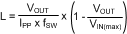
 Figure 8-2 Inductor Current
The maximum ripple current occurs at the maximum input voltage. Typically, IPP is selected between 20% and 40% of the full load current. Higher ripple current results in a smaller inductor. However, it places more burden on the output capacitor to smooth out the ripple current to achieve low output ripple voltage. For this example, 40% ripple was chosen for a smaller sized inductor.
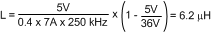
The nearest standard value of 6.8 µH is used. To prevent saturation, the inductor must be rated for the peak current. During normal operation, the peak current occurs at maximum load current (plus maximum ripple). With properly scaled component values, the peak current is limited to VCS(TH) / RS during overload conditions. At the maximum input voltage with a shorted output, the chosen inductor must be evaluated at elevated temperature. Note that the saturation current rating of inductors drops significantly at elevated temperatures.