SNVSAP9A March   2017  – February 2018 LM25141-Q1

PRODUCTION DATA.  

  1. Features
  2. Applications
  3. Description
    1.     Device Images
      1.      Simplified Schematic
  4. Revision History
  5. Pin Configuration and Functions
    1.     Pin Functions
  6. Specifications
    1. 6.1 Absolute Maximum Ratings
    2. 6.2 ESD Ratings
    3. 6.3 Recommended Operating Conditions
    4. 6.4 Thermal Information
    5. 6.5 Electrical Characteristics
    6. 6.6 Switching Characteristics
    7. 6.7 Typical Characteristics
  7. Detailed Description
    1. 7.1 Overview
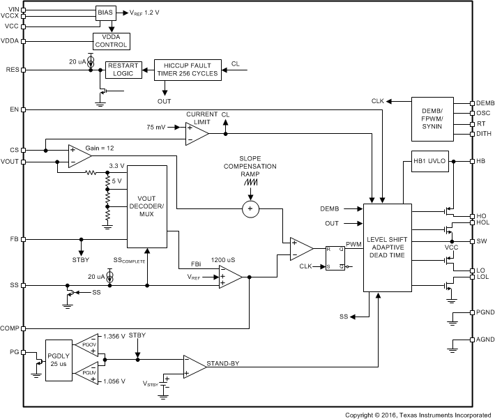
    2. 7.2 Functional Block Diagram
    3. 7.3 Feature Description
      1. 7.3.1  High Voltage Start-Up Regulator
      2. 7.3.2  VCC Regulator
      3. 7.3.3  Oscillator
      4. 7.3.4  Synchronization
      5. 7.3.5  Frequency Dithering (Spread Spectrum)
      6. 7.3.6  Enable
      7. 7.3.7  Power Good
      8. 7.3.8  Output Voltage
        1. 7.3.8.1 Minimum Output Voltage Adjustment
      9. 7.3.9  Current Sense
      10. 7.3.10 DCR Current Sensing
      11. 7.3.11 Error Amplifier and PWM Comparator
      12. 7.3.12 Slope Compensation
      13. 7.3.13 Hiccup Mode Current Limiting
      14. 7.3.14 Standby Mode
      15. 7.3.15 Soft Start
      16. 7.3.16 Diode Emulation
      17. 7.3.17 High- and Low-Side Drivers
  8. Application and Implementation
    1. 8.1 Application Information
    2. 8.2 Typical Application
      1. 8.2.1 Design Requirements
      2. 8.2.2 Detailed Design Procedure
        1. 8.2.2.1 Custom Design With WEBENCH® Tools
        2. 8.2.2.2 Inductor Calculation
        3. 8.2.2.3 Current Sense Resistor
        4. 8.2.2.4 Output Capacitor
        5. 8.2.2.5 Input Filter
          1. 8.2.2.5.1 EMI Filter Design
          2. 8.2.2.5.2 MOSFET Selection
          3. 8.2.2.5.3 Driver Slew Rate Control
          4. 8.2.2.5.4 Frequency Dithering
        6. 8.2.2.6 Control Loop
          1. 8.2.2.6.1 Feedback Compensator
      3. 8.2.3 Application Curves
  9. Power Supply Recommendations
  10. 10Layout
    1. 10.1 Layout Guidelines
      1. 10.1.1 Layout Procedure
    2. 10.2 Layout Examples
  11. 11Device and Documentation Support
    1. 11.1 Device Support
      1. 11.1.1 Development Support
        1. 11.1.1.1 Custom Design With WEBENCH® Tools
    2. 11.2 Documentation Support
      1. 11.2.1 Related Documentation
        1. 11.2.1.1 PCB Layout Resources
        2. 11.2.1.2 Thermal Design Resources
    3. 11.3 Receiving Notification of Documentation Updates
    4. 11.4 Community Resources
    5. 11.5 Trademarks
    6. 11.6 Electrostatic Discharge Caution
    7. 11.7 Glossary
  12. 12Mechanical, Packaging, and Orderable Information

Package Options

Mechanical Data (Package|Pins)
Thermal pad, mechanical data (Package|Pins)
Orderable Information

Functional Block Diagram

LM25141-Q1 fbd_SNVSAP9.gif