SNVSB79B November   2018  – May 2020 LM25180

PRODUCTION DATA.  

  1. Features
  2. Applications
  3. Description
    1.     Device Images
      1.      Typical Application
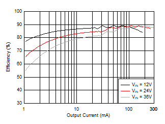
      2.      Typical Efficiency, VOUT = 5 V
  4. Revision History
  5. Description (continued)
  6. Pin Configuration and Functions
    1.     Pin Functions
  7. Specifications
    1. 7.1 Absolute Maximum Ratings
    2. 7.2 ESD Ratings
    3. 7.3 Recommended Operating Conditions
    4. 7.4 Thermal Information
    5. 7.5 Electrical Characteristics
    6. 7.6 Typical Characteristics
  8. Detailed Description
    1. 8.1 Overview
    2. 8.2 Functional Block Diagram
    3. 8.3 Feature Description
      1. 8.3.1  Integrated Power MOSFET
      2. 8.3.2  PSR Flyback Modes of Operation
      3. 8.3.3  Setting the Output Voltage
        1. 8.3.3.1 Diode Thermal Compensation
      4. 8.3.4  Control Loop Error Amplifier
      5. 8.3.5  Precision Enable
      6. 8.3.6  Configurable Soft Start
      7. 8.3.7  External Bias Supply
      8. 8.3.8  Minimum On-Time and Off-Time
      9. 8.3.9  Overcurrent Protection
      10. 8.3.10 Thermal Shutdown
    4. 8.4 Device Functional Modes
      1. 8.4.1 Shutdown Mode
      2. 8.4.2 Standby Mode
      3. 8.4.3 Active Mode
  9. Application and Implementation
    1. 9.1 Application Information
    2. 9.2 Typical Applications
      1. 9.2.1 Design 1: Wide VIN, Low IQ PSR Flyback Converter Rated at 5 V, 1 A
        1. 9.2.1.1 Design Requirements
        2. 9.2.1.2 Detailed Design Procedure
          1. 9.2.1.2.1  Custom Design With WEBENCH® Tools
          2. 9.2.1.2.2  Custom Design With Excel Quickstart Tool
          3. 9.2.1.2.3  Flyback Transformer – T1
          4. 9.2.1.2.4  Flyback Diode – DFLY
          5. 9.2.1.2.5  Zener Clamp Circuit – DF, DCLAMP
          6. 9.2.1.2.6  Output Capacitor – COUT
          7. 9.2.1.2.7  Input Capacitor – CIN
          8. 9.2.1.2.8  Feedback Resistor – RFB
          9. 9.2.1.2.9  Thermal Compensation Resistor – RTC
          10. 9.2.1.2.10 UVLO Resistors – RUV1, RUV2
          11. 9.2.1.2.11 Soft-Start Capacitor – CSS
        3. 9.2.1.3 Application Curves
      2. 9.2.2 Design 2: PSR Flyback Converter With Dual Outputs of 15 V and –7.7 V at 200 mA
        1. 9.2.2.1 Design Requirements
        2. 9.2.2.2 Detailed Design Procedure
          1. 9.2.2.2.1 Flyback Transformer – T1
          2. 9.2.2.2.2 Flyback Diodes – DFLY1 and DFLY2
          3. 9.2.2.2.3 Input Capacitor – CIN
          4. 9.2.2.2.4 Feedback Resistor – RFB
          5. 9.2.2.2.5 UVLO Resistors – RUV1, RUV2
        3. 9.2.2.3 Application Curves
      3. 9.2.3 Design 3: PSR Flyback Converter With Stacked Dual Outputs of 24 V and 5 V
        1. 9.2.3.1 Design Requirements
        2. 9.2.3.2 Detailed Design Procedure
          1. 9.2.3.2.1 Flyback Transformer – T1
          2. 9.2.3.2.2 Feedback Resistor – RFB
          3. 9.2.3.2.3 UVLO Resistors – RUV1, RUV2
        3. 9.2.3.3 Application Curves
  10. 10Power Supply Recommendations
  11. 11Layout
    1. 11.1 Layout Guidelines
    2. 11.2 Layout Examples
  12. 12Device and Documentation Support
    1. 12.1 Device Support
      1. 12.1.1 Third-Party Products Disclaimer
      2. 12.1.2 Development Support
      3. 12.1.3 Custom Design With WEBENCH® Tools
    2. 12.2 Documentation Support
      1. 12.2.1 Related Documentation
    3. 12.3 Receiving Notification of Documentation Updates
    4. 12.4 Support Resources
    5. 12.5 Trademarks
    6. 12.6 Electrostatic Discharge Caution
    7. 12.7 Glossary
  13. 13Mechanical, Packaging, and Orderable Information

Package Options

Refer to the PDF data sheet for device specific package drawings

Mechanical Data (Package|Pins)
  • NGU|8
Thermal pad, mechanical data (Package|Pins)
Orderable Information

Application Curves

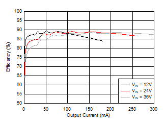
LM25180 D016_snvsb06.gifFigure 35. Efficiency (Linear Scale)
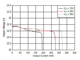
LM25180 D017_snvsb06.gif
Total of VOUT1 and VOUT2
Figure 37. Load Regulation (Linear Scale)
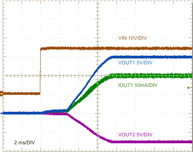
LM25180 LM5180_design2_startup_waveform_nvsb06.gif
VIN stepped to 24 V 75 Ω and 40 Ω Loads
Figure 39. Start-Up Characteristic
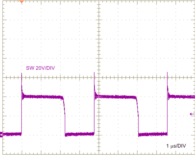
LM25180 LM5180_design2_SWnode24Vin_waveform_nvsb06.gif
VIN = 24 V
Figure 41. Switch Voltage, Full Load
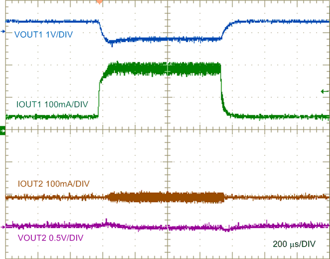
LM25180 LM5180_design2_load1_transient_waveform_nvsb06.gif
VIN = 24 V IOUT1 = 200 mA
Figure 43. Output 1 Load Transient, 50 mA to 200 mA
LM25180 D015_snvsb06.gifFigure 36. Efficiency (Log Scale)
LM25180 D018_snvsb06.gif
Total of VOUT1 and VOUT2
Figure 38. Load Regulation (Log Scale)
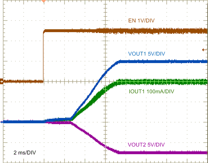
LM25180 LM5180_design2_ENstartup_waveform_nvsb06.gif
VIN = 24 V 75 Ω and 40 Ω Loads
Figure 40. ENABLE ON Characteristic
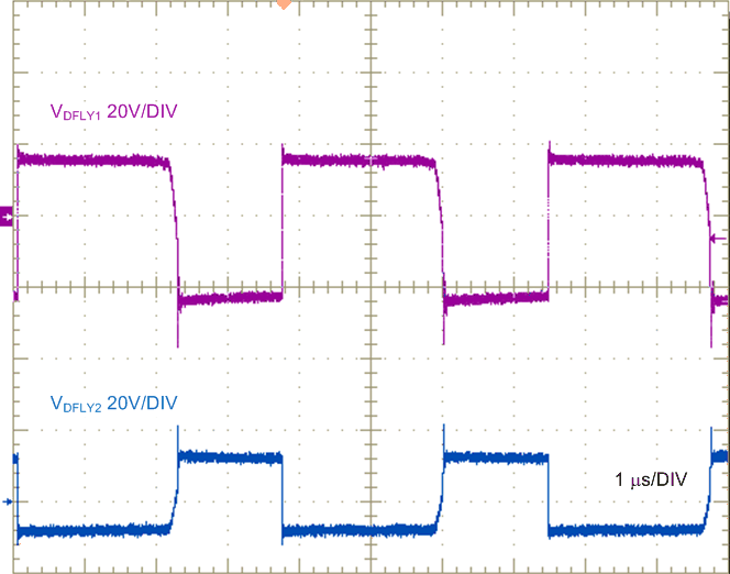
LM25180 LM5180_design2_24V_VD_waveform_nvsb06.gif
VIN = 24 V
Figure 42. Flyback Diode Voltages, Full Load
LM25180 LM5180_design2_load2_transient_waveform_nvsb06.gif
VIN = 24 V IOUT2 = 200 mA
Figure 44. Output 2 Load Transient, 50 mA to 200 mA