SLVS569F January 2005 – August 2015 LM2575
PRODUCTION DATA.
- 1 Features
- 2 Applications
- 3 Description
- 4 Revision History
- 5 Pin Configuration and Functions
- 6 Specifications
- 7 Detailed Description
-
8 Application and Implementation
- 8.1 Application Information
- 8.2
Typical Application
- 8.2.1 Design Requirements
- 8.2.2
Detailed Design Procedure
- 8.2.2.1 Input Capacitor (CIN)
- 8.2.2.2 Output Capacitor (COUT)
- 8.2.2.3 Catch Diode
- 8.2.2.4 Inductor
- 8.2.2.5 Output Voltage Ripple and Transients
- 8.2.2.6 Feedback Connection
- 8.2.2.7 ON/OFF Input
- 8.2.2.8 Grounding
- 8.2.2.9 Reverse Current Considerations
- 8.2.2.10 Buck Regulator Design Procedure
- 8.2.2.11 Inductor Selection Guide
- 8.2.3 Application Curves
- 9 Power Supply Recommendations
- 10Layout
- 11Device and Documentation Support
- 12Mechanical, Packaging, and Orderable Information
Package Options
Refer to the PDF data sheet for device specific package drawings
Mechanical Data (Package|Pins)
- N|16
Thermal pad, mechanical data (Package|Pins)
Orderable Information
7 Detailed Description
7.1 Overview
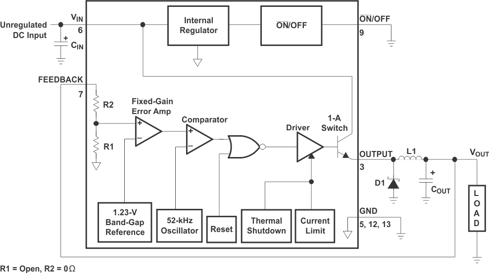
The LM2575 provides all the active functions needed for a step-down (buck) switching regulator in an integrated circuit. The wide input-voltage range is 4.75 V to 40 V. The output voltage is programmable by two external resistors. No external frequency compensation is needed. The integrated switch is capable of delivering 1 A of load current, with excellent line and load regulation. The fixed 52-kHz output has cycle-by-cycle current limiting, and thermal shutdown. In addition, a manual shutdown is available through an external ON/OFF pin.
The LM2575 is characterized for operation over the virtual junction temperature range of –40°C to 125°C.
7.2 Functional Block Diagram

7.3 Feature Description
7.3.1 Feedback Connection
FEEDBACK must be connected between the two programming resistors. Again, both of these resistors must be in close proximity to the regulator, and each must be less than 100 kΩ to minimize noise pickup.
7.3.2 ON/OFF Input
ON/OFF should be grounded or be a low-level TTL voltage (typically < 1.6 V) for normal operation. To shut down the LM2575 device and place in standby mode, a high-level TTL or CMOS voltage should be supplied to this pin. ON/OFF must not be left open and safely can be pulled up to VIN with or without a pullup resistor.
7.3.3 Fault Protection
In the event of an output short or an overload condition, self-protection features lower the oscillator frequency to approximately 18 kHz and the minimum duty cycle from 5% to approximately 2%. The resulting output voltage drops to approximately 40% of its nominal value, causing the average power dissipated by the IC to lower.
7.4 Device Functional Modes
7.4.1 Normal Operation Mode
When a low-level TTL or CMOS voltage is applied to the ON/OFF pin, the device will provide an output voltage.
7.4.2 Standby Mode
When a high-level TTL or CMOS voltage is applied to the ON/OFF pin, the device enters standby mode, drawing a typical quiescent current of 50 µA. The internal output switch will be turned off.