SNVS117E April   1998  – June 2019 LM2588

PRODUCTION DATA.  

  1. Features
  2. Typical Applications
  3. Description
    1.     Device Images
      1.      Flyback Regulator
  4. Revision History
  5. Pin Configurations
  6. Specifications
    1. 6.1 Absolute Maximum Ratings
    2. 6.2 ESD Ratings
    3. 6.3 Recommended Operating Ratings
    4. 6.4 Electrical Characteristics: 3.3 V
    5. 6.5 Electrical Characteristics: 5 V
    6. 6.6 Electrical Characteristics: 12 V
    7. 6.7 Electrical Characteristics: Adjustable
    8. 6.8 Electrical Characteristics: All Output Voltage Versions
    9. 6.9 Typical Characteristics
  7. Detailed Description
    1. 7.1 Overview
    2. 7.2 Functional Block Diagram
    3. 7.3 Feature Description
      1. 7.3.1 Flyback Regulator Operation
      2. 7.3.2 Step-Up (Boost) Regulator Operation
      3. 7.3.3 Shutdown Control
      4. 7.3.4 Frequency Adjustment
      5. 7.3.5 Frequency Synchronization
      6. 7.3.6 Programming Output Voltage (Selecting R1 And R2)
      7. 7.3.7 Short-Circuit Condition
  8. Application and Implementation
    1. 8.1 Application Information
    2. 8.2 Typical Applications
      1. 8.2.1 Typical Flyback Regulator Applications
        1. 8.2.1.1 Design Requirements
          1. 8.2.1.1.1 Transformer Selection (T)
          2. 8.2.1.1.2 Transformer Footprints
        2. 8.2.1.2 Detailed Design Procedure
          1. 8.2.1.2.1 Custom Design With WEBENCH® Tools
          2. 8.2.1.2.2 Flyback Regulator Input Capacitors
          3. 8.2.1.2.3 Switch Voltage Limits
          4. 8.2.1.2.4 Output Voltage Limitations
          5. 8.2.1.2.5 Noisy Input Line Condition
          6. 8.2.1.2.6 Stability
      2. 8.2.2 Typical Boost Regulator Applications
        1. 8.2.2.1 Design Requirements
        2. 8.2.2.2 Detailed Design Procedure
    3. 8.3 System Examples
      1. 8.3.1 Test Circuits
  9. Layout
    1. 9.1 Layout Guidelines
    2. 9.2 Layout Example
    3. 9.3 Heat Sink/Thermal Considerations
  10. 10Device and Documentation Support
    1. 10.1 Device Support
      1. 10.1.1 Third-Party Products Disclaimer
      2. 10.1.2 Development Support
        1. 10.1.2.1 Custom Design With WEBENCH® Tools
    2. 10.2 Receiving Notification of Documentation Updates
    3. 10.3 Community Resources
    4. 10.4 Trademarks
    5. 10.5 Electrostatic Discharge Caution
    6. 10.6 Glossary
  11. 11Mechanical, Packaging, and Orderable Information

Package Options

Mechanical Data (Package|Pins)
Thermal pad, mechanical data (Package|Pins)
Orderable Information

Shutdown Control

A feature of the LM2588 is its ability to be shut down using the ON /OFF pin (pin 1). This feature conserves input power by turning off the device when it is not in use. For proper operation, an isolation diode is required (as shown in Figure 20).

The device will shut down when 3 V or greater is applied on the ON /OFF pin, sourcing current into pin 1. In shut down mode, the device draws typically 56 μA of supply current (16 μA to VIN and 40 μA to the ON /OFF pin). To turn the device back on, leave pin 1 floating, using an (isolation) diode, as shown in Figure 20 (for normal operation, do not source or sink current to or from this pin—see the next section).
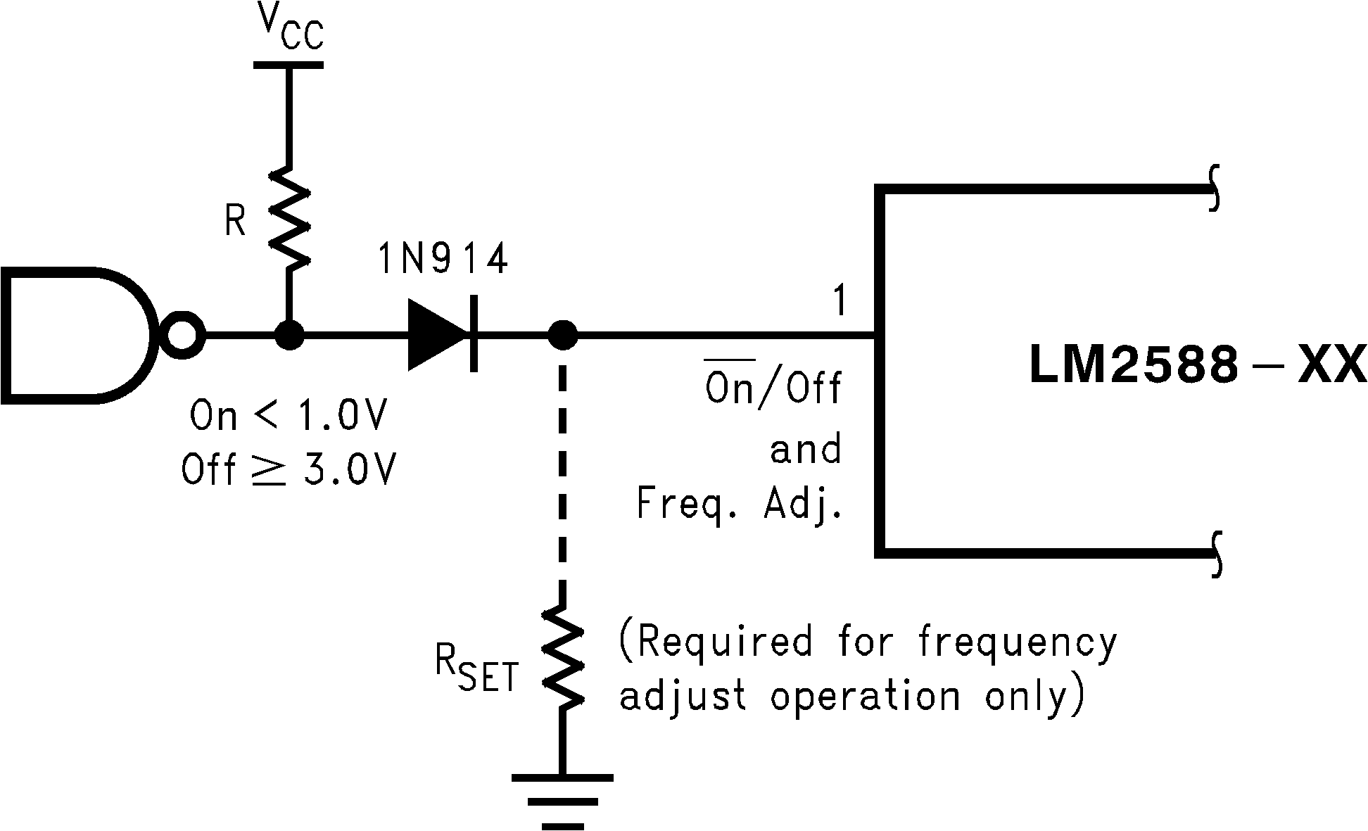
LM2588 01242054.pngFigure 20. Shutdown Operation