SNVS074E May 2001 – May 2016 LM2591HV
PRODUCTION DATA.
- 1 Features
- 2 Applications
- 3 Description
- 4 Revision History
- 5 Description (continued)
- 6 Pin Configuration and Functions
-
7 Specifications
- 7.1 Absolute Maximum Ratings
- 7.2 ESD Ratings
- 7.3 Recommended Operating Conditions
- 7.4 Thermal Information
- 7.5 Electrical Characteristics LM2591HV-3.3
- 7.6 Electrical Characteristics LM2591HV-5.0
- 7.7 Electrical Characteristics LM2591HV-ADJ
- 7.8 Electrical Characteristics All Output Voltage Versions
- 7.9 Typical Characteristics
- 8 Parameter Measurement Information
- 9 Detailed Description
- 10Application and Implementation
- 11Power Supply Recommendations
- 12Layout
- 13Device and Documentation Support
- 14Mechanical, Packaging, and Orderable Information
Package Options
Mechanical Data (Package|Pins)
Thermal pad, mechanical data (Package|Pins)
- KTT|5
Orderable Information
8 Parameter Measurement Information
8.1 Test Circuits

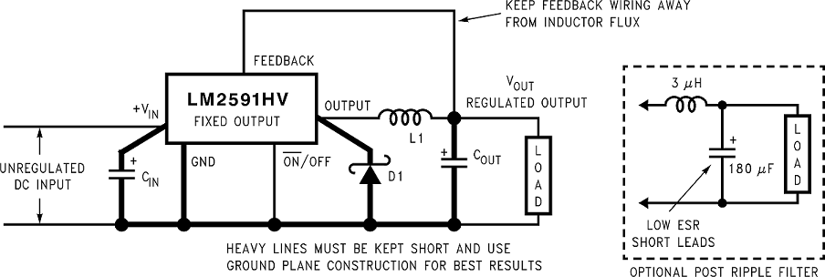
Component Values shown are for VIN = 15V,
VOUT = 5V, ILOAD = 1A.
CIN — 470 μF, 50V, Aluminum Electrolytic Nichicon “PM Series”
COUT — 220 μF, 25V Aluminum Electrolytic, Nichicon “PM Series”
D1 — 2A, 60V Schottky Rectifier, 21DQ06 (International Rectifier)
L1 — 68 H, See Inductor Selection Procedure
Figure 19. Fixed Output Voltage Versions
VOUT = 5V, ILOAD = 1A.
CIN — 470 μF, 50V, Aluminum Electrolytic Nichicon “PM Series”
COUT — 220 μF, 25V Aluminum Electrolytic, Nichicon “PM Series”
D1 — 2A, 60V Schottky Rectifier, 21DQ06 (International Rectifier)
L1 — 68 H, See Inductor Selection Procedure

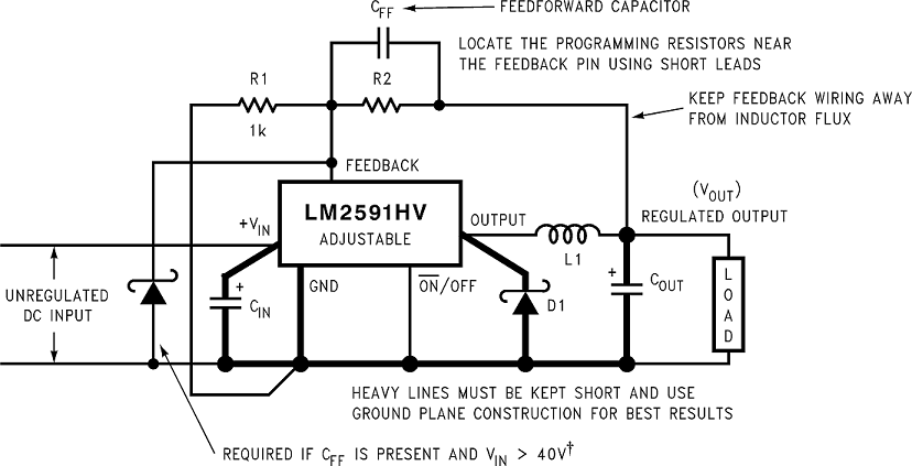
Select R1 to be approximately 1 kΩ, use a 1% resistor for best stability.
Component Values shown are for VIN = 20V,
VOUT = 10V, ILOAD = 1A.
CIN: — 470 μF, 35V, Aluminum Electrolytic Nichicon “PM Series”
COUT: — 220 μF, 35V Aluminum Electrolytic, Nichicon “PM Series”
D1 — 2A, 60V Schottky Rectifier, 21DQ06 (International Rectifier)
See Inductor Selection Procedure L1 — 100 μH,
R1 — 1 kΩ, 1%
R2 — 7.15k, 1%
CFF — 3.3 nF
Typical Values
CSS—0.1 μF
CDELAY—0.1 μF
RPULL UP — 4.7k (use 22k if VOUT is ≥ 45V)
† Small signal Schottky diode to prevent damage to feedback pin by negative spike when output is shorted. Required if VIN > 40V
Figure 20. Adjustable Output Voltage Versions
Component Values shown are for VIN = 20V,
VOUT = 10V, ILOAD = 1A.
CIN: — 470 μF, 35V, Aluminum Electrolytic Nichicon “PM Series”
COUT: — 220 μF, 35V Aluminum Electrolytic, Nichicon “PM Series”
D1 — 2A, 60V Schottky Rectifier, 21DQ06 (International Rectifier)
See Inductor Selection Procedure L1 — 100 μH,
R1 — 1 kΩ, 1%
R2 — 7.15k, 1%
CFF — 3.3 nF
Typical Values
CSS—0.1 μF
CDELAY—0.1 μF
RPULL UP — 4.7k (use 22k if VOUT is ≥ 45V)
† Small signal Schottky diode to prevent damage to feedback pin by negative spike when output is shorted. Required if VIN > 40V