SNVS122C May 1999 – May 2016 LM2595
PRODUCTION DATA.
- 1 Features
- 2 Applications
- 3 Description
- 4 Revision History
- 5 Description (continued)
- 6 Pin Configuration and Functions
-
7 Specifications
- 7.1 Absolute Maximum Ratings
- 7.2 ESD Ratings
- 7.3 Recommended Operating Conditions
- 7.4 Thermal Information
- 7.5 Electrical Characteristics - 3.3 V
- 7.6 Electrical Characteristics - 5 V
- 7.7 Electrical Characteristics - 12 V
- 7.8 Electrical Characteristics - Adjustable
- 7.9 Electrical Characteristics - All Output Voltage Versions
- 7.10 Typical Characteristics
- 8 Detailed Description
- 9 Application and Implementation
- 10Power Supply Recommendations
- 11Layout
- 12Device and Documentation Support
- 13Mechanical, Packaging, and Orderable Information
Package Options
Refer to the PDF data sheet for device specific package drawings
Mechanical Data (Package|Pins)
- NDH|5
- KTT|5
Thermal pad, mechanical data (Package|Pins)
- KTT|5
Orderable Information
8 Detailed Description
8.1 Overview
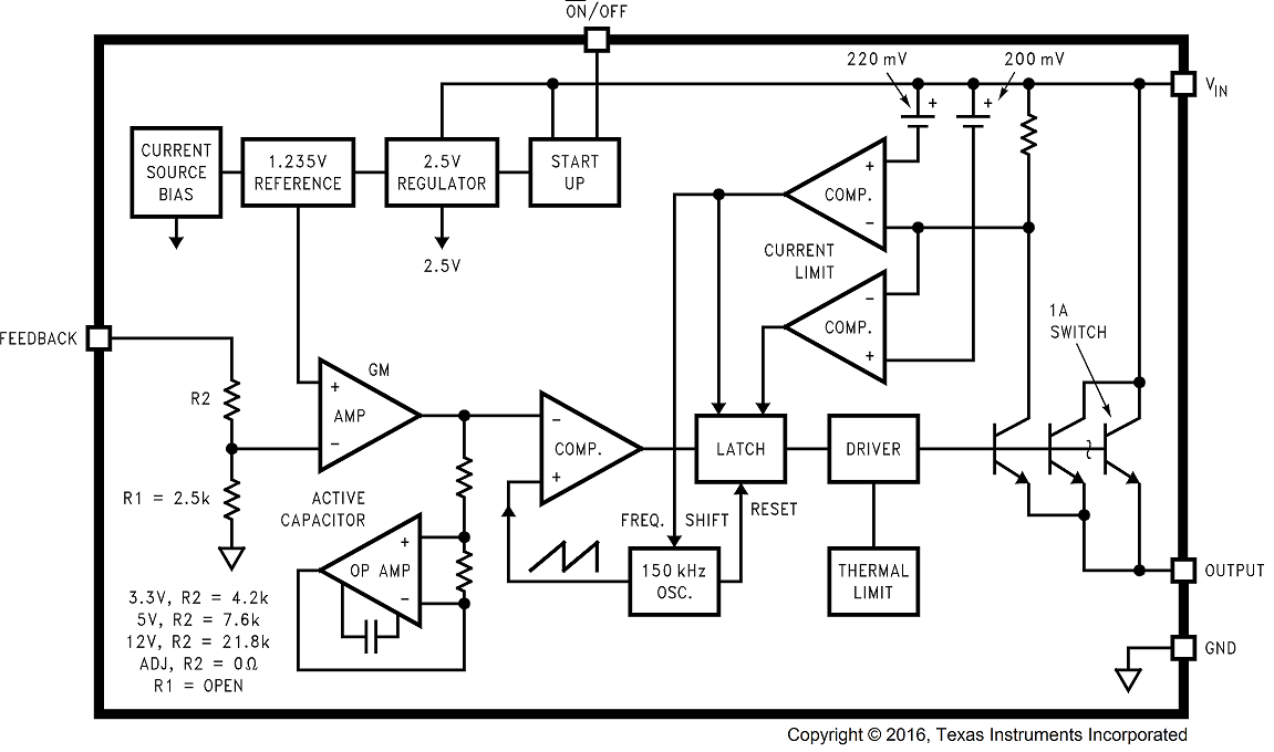
The LM2595 SIMPLE SWITCHER® regulator is an easy-to-use, nonsynchronous step-down DC-DC converter with a wide input voltage range up to 40 V. The regulator is capable of delivering up to 1-A DC load current with excellent line and load regulation. These devices are available in fixed output voltages of 3.3-V, 5-V, 12-V, and an adjustable output version. The family requires few external components, and the pin arrangement was designed for simple, optimum PCB layout.
8.2 Functional Block Diagram
8.3 Feature Description
8.3.1 Delayed Start-Up
The circuit in Figure 14 uses the ON/OFF pin to provide a time delay between the time the input voltage is applied and the time the output voltage comes up (only the circuitry pertaining to the delayed start up is shown). As the input voltage rises, the charging of capacitor C1 pulls the ON/OFF pin high, keeping the regulator off. Once the input voltage reaches its final value and the capacitor stops charging, the resistor R2 pulls the ON/OFF pin low, thus allowing the circuit to start switching. Resistor R1 is included to limit the maximum voltage applied to the ON/OFF pin (maximum of 25 V), reduces power supply noise sensitivity, and also limits the capacitor, C1, discharge current. When high input ripple voltage exists, avoid long delay time, because this ripple can be coupled into the ON/OFF pin and cause problems.
This delayed start-up feature is useful in situations where the input power source is limited in the amount of current it can deliver. It allows the input voltage to rise to a higher voltage before the regulator starts operating. Buck regulators require less input current at higher input voltages.
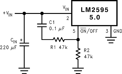 Figure 14. Delayed Start-Up
8.3.2 Undervoltage Lockout
Some applications require the regulator to remain off until the input voltage reaches a predetermined voltage. Figure 15 shows an undervoltage lockout feature applied to a buck regulator, while Figure 16 and Figure 17 apply the same feature to an inverting circuit. The circuit in Figure 16 features a constant threshold voltage for turnon and turnoff (Zener voltage plus approximately one volt). If hysteresis is required, the circuit in Figure 17 has a turnon voltage which is different than the turnoff voltage. The amount of hysteresis is approximately equal to the value of the output voltage. If Zener voltages greater than 25 V are used, an additional 47-kΩ resistor is required from the ON/OFF pin to the ground pin to stay within the 25-V maximum limit of the ON/OFF pin.
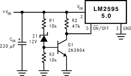 Figure 15. Undervoltage Lockout for Buck Regulator
8.3.3 Inverting Regulator
The circuit in Figure 18 converts a positive input voltage to a negative output voltage with a common ground. The circuit operates by bootstrapping the regulator's ground pin to the negative output voltage, then grounding the feedback pin, the regulator senses the inverted output voltage and regulates it.
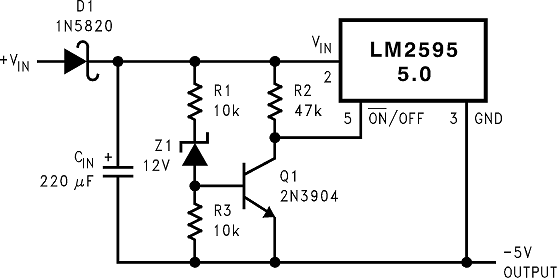
This example uses the LM2595 5-V version to generate a −5-V output, but other output voltages are possible by selecting other output voltage versions, including the adjustable version.
Because this regulator topology can produce an output voltage that is either greater than or less than the input voltage, the maximum output current greatly depends on both the input and output voltage. Figure 19 provides a guide as to the amount of output load current possible for the different input and output voltage conditions.
The maximum voltage appearing across the regulator is the absolute sum of the input and output voltage, and this must be limited to a maximum of 40 V. For example, when converting 20 V to −12 V, the regulator would see 32 V between the input pin and ground pin. The LM2595 has a maximum input voltage spec of 40 V.
Additional diodes are required in this regulator configuration. Diode D1 is used to isolate input voltage ripple or noise from coupling through the CIN capacitor to the output, under light or no load conditions. Also, this diode isolation changes the topology to closely resemble a buck configuration thus providing good closed loop stability. TI recommends a Schottky diode for low input voltages (because of its lower voltage drop), but for higher input voltages, a fast recovery diode could be used.
Without diode D3, when the input voltage is first applied, the charging current of CIN can pull the output positive by several volts for a short period of time. Adding D3 prevents the output from going positive by more than a diode voltage.

Regulator starts switching at VIN = 13 V
Regulator stops switching at VIN = 8 V

120-μF, 50-V electrolytic Panasonic HFQ
COUT – 22-μF, 20-V tantalum Sprague 595D
120-μF, 25-V electrolytic Panasonic HFQ
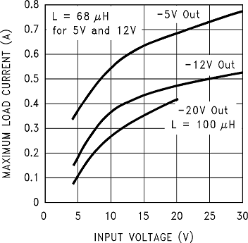 Figure 19. Inverting Regulator Typical Load Current
Because of differences in the operation of the inverting regulator, the standard design procedure is not used to select the inductor value. In the majority of designs, a 68-μH, 1.5-A inductor is the best choice. Capacitor selection is narrowed down to just a few values. Using the values shown in Figure 18 will provide good results in the majority of inverting designs.
This type of inverting regulator can require relatively large amounts of input current when starting up, even with light loads. Input currents as high as the LM2595 current limit (approximately 1.5 A) are required for at least 2 ms or more, until the output reaches its nominal output voltage. The actual time depends on the output voltage and the size of the output capacitor. Input power sources that are current limited or sources that can not deliver these currents without getting loaded down, may not work correctly. Because of the relatively high start-up currents required by the inverting topology, the delayed start-up feature (C1, R1 and R2) shown in Figure 18 is recommended. By delaying the regulator start-up, the input capacitor is allowed to charge up to a higher voltage before the switcher begins operating. A portion of the high input current required for start-up is now supplied by the input capacitor (CIN). For severe start up conditions, the input capacitor can be made much larger than normal.
8.3.4 Inverting Regulator Shutdown Methods
Using the ON/OFF pin in a standard buck configuration is simple. To turn the regulator ON, pull the ON/OFF pin below 1.3 V (at 25°C referenced to ground). To shut the regulator OFF, pull the ON/OFF pin above 1.3 V. With the inverting configuration, some level shifting is required, because the ground pin of the regulator is no longer at ground, but is now setting at the negative output voltage level. Two different shutdown methods for inverting regulators are shown in Figure 20 and Figure 21.
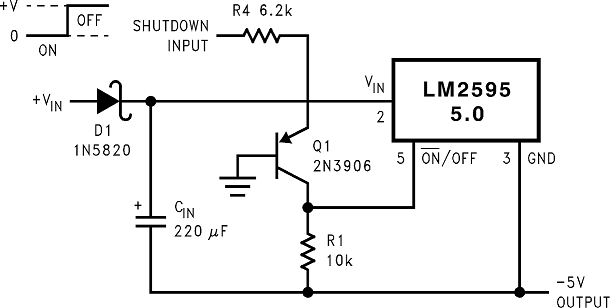 Figure 20. Inverting Regulator Ground Referenced Shutdown
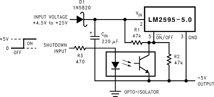 Figure 21. Inverting Regulator Ground Referenced Shutdown Using Opto Device
8.4 Device Functional Modes
8.4.1 Discontinuous Mode Operation
The selection guide chooses inductor values suitable for continuous mode operation, but for low current applications or high input voltages, a discontinuous mode design may be a better choice. Discontinuous mode would use an inductor that would be physically smaller, and would need only one half to one third the inductance value required for a continuous mode design. The peak switch and inductor currents will be higher in a discontinuous design, but at these low load currents (400 mA and below), the maximum switch current will still be less than the switch current limit.
Discontinuous operation can have voltage waveforms that are considerably different than a continuous design. The output pin (switch) waveform can have some damped sinusoidal ringing present (see Typical Characteristics). This ringing is normal for discontinuous operation, and is not caused by feedback loop instabilities. In discontinuous operation, there is a period of time where neither the switch nor the diode are conducting, and the inductor current has dropped to zero. During this time, a small amount of energy can circulate between the inductor and the switch/diode parasitic capacitance causing this characteristic ringing. Normally this ringing is not a problem, unless the amplitude becomes great enough to exceed the input voltage, and even then, there is very little energy present to cause damage.
Different inductor types and/or core materials produce different amounts of this characteristic ringing. Ferrite core inductors have very little core loss and therefore produce the most ringing. The higher core loss of powdered iron inductors produce less ringing. If desired, a series RC could be placed in parallel with the inductor to dampen the ringing.
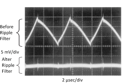 Figure 22. Post Ripple Filter Waveform