SNVS122C May 1999 – May 2016 LM2595
PRODUCTION DATA.
- 1 Features
- 2 Applications
- 3 Description
- 4 Revision History
- 5 Description (continued)
- 6 Pin Configuration and Functions
-
7 Specifications
- 7.1 Absolute Maximum Ratings
- 7.2 ESD Ratings
- 7.3 Recommended Operating Conditions
- 7.4 Thermal Information
- 7.5 Electrical Characteristics - 3.3 V
- 7.6 Electrical Characteristics - 5 V
- 7.7 Electrical Characteristics - 12 V
- 7.8 Electrical Characteristics - Adjustable
- 7.9 Electrical Characteristics - All Output Voltage Versions
- 7.10 Typical Characteristics
- 8 Detailed Description
- 9 Application and Implementation
- 10Power Supply Recommendations
- 11Layout
- 12Device and Documentation Support
- 13Mechanical, Packaging, and Orderable Information
Package Options
Refer to the PDF data sheet for device specific package drawings
Mechanical Data (Package|Pins)
- NDH|5
- KTT|5
Thermal pad, mechanical data (Package|Pins)
- KTT|5
Orderable Information
9 Application and Implementation
NOTE
Information in the following applications sections is not part of the TI component specification, and TI does not warrant its accuracy or completeness. TI’s customers are responsible for determining suitability of components for their purposes. Customers should validate and test their design implementation to confirm system functionality.
9.1 Application Information
9.1.1 Input Capacitor (CIN)
A low ESR aluminum or tantalum bypass capacitor is required between the input pin and ground pin. The capacitor must be placed near the regulator using short leads. This capacitor prevents large voltage transients from appearing at the input, and provides the instantaneous current required each time the switch turns on.
The important parameters for the Input capacitor are the voltage rating and the RMS current rating. Because of the relatively high RMS currents flowing in a buck regulator's input capacitor, this capacitor must be chosen for its RMS current rating rather than its capacitance or voltage ratings, although the capacitance value and voltage rating are directly related to the RMS current rating.
The RMS current rating of a capacitor could be viewed as a capacitor's power rating. The RMS current flowing through the capacitors internal ESR produces power which causes the internal temperature of the capacitor to rise. The RMS current rating of a capacitor is determined by the amount of current required to raise the internal temperature approximately 10°C above an ambient temperature of 105°C. The ability of the capacitor to dissipate this heat to the surrounding air will determine the amount of current the capacitor can safely sustain. Capacitors that are physically large and have a large surface area will typically have higher RMS current ratings. For a given capacitor value, a higher voltage electrolytic capacitor will be physically larger than a lower voltage capacitor, and thus be able to dissipate more heat to the surrounding air, and therefore will have a higher RMS current rating.
The consequences of operating an electrolytic capacitor above the RMS current rating is a shortened operating life. The higher temperature speeds up the evaporation of the capacitor's electrolyte, resulting in eventual failure.
Selecting an input capacitor requires consulting the manufacturer's data sheet for maximum allowable RMS ripple current. For a maximum ambient temperature of 40°C, a general guideline would be to select a capacitor with a ripple current rating of approximately 50% of the DC load current. For ambient temperatures up to 70°C, a current rating of 75% of the DC load current would be a good choice for a conservative design. The capacitor voltage rating must be at least 1.25 times greater than the maximum input voltage, and often a much higher voltage capacitor is required to satisfy the RMS current requirements.
Figure 23 shows the relationship between an electrolytic capacitor value, its voltage rating, and the RMS current it is rated for. These curves were obtained from the Nichicon PL series of low-ESR, high-reliability electrolytic capacitors designed for switching regulator applications. Other capacitor manufacturers offer similar types of capacitors, but always check the capacitor data sheet.
Standard electrolytic capacitors typically have much higher ESR numbers, lower RMS current ratings and typically have a shorter operating lifetime.
Because of their small size and excellent performance, surface-mount solid tantalum capacitors are often used for input bypassing, but several precautions must be observed. A small percentage of solid tantalum capacitors can short if the inrush current rating is exceeded. This can happen at turnon when the input voltage is suddenly applied, and of course, higher input voltages produce higher inrush currents. Several capacitor manufacturers do a 100% surge current testing on their products to minimize this potential problem. If high turn on currents are expected, it may be necessary to limit this current by adding either some resistance or inductance before the tantalum capacitor, or select a higher voltage capacitor. As with aluminum electrolytic capacitors, the RMS ripple current rating must be sized to the load current.
9.1.2 Feedforward Capacitor (CFF) for Adjustable Output Voltage Version Only
A feedforward capacitor, CFF, shown across R2 in Table 1 is used when the output voltage is greater than 10 V or when COUT has a very low ESR. This capacitor adds lead compensation to the feedback loop and increases the phase margin for better loop stability.
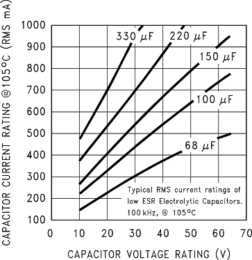 Figure 23. RMS Current Ratings for Low ESR Electrolytic Capacitors (Typical)
9.1.3 Output Capacitor (COUT)
An output capacitor is required to filter the output and provide regulator loop stability. Low impedance or low ESR Electrolytic or solid tantalum capacitors designed for switching regulator applications must be used. When selecting an output capacitor, the important capacitor parameters are the 100-kHz Equivalent Series Resistance (ESR), the RMS ripple current rating, voltage rating, and capacitance value. For the output capacitor, the ESR value is the most important parameter.
The output capacitor requires an ESR value that has an upper and lower limit. For low output ripple voltage, a low ESR value is required. This value is determined by the maximum allowable output ripple voltage, typically 1% to 2% of the output voltage. But if the selected capacitor's ESR is extremely low, there is a possibility of an unstable feedback loop, resulting in an oscillation at the output. Using the capacitors listed in the tables, or similar types, will provide design solutions under all conditions.
If very low output ripple voltage (less than 15 mV) is required, see Output Voltage Ripple and Transients for a post ripple filter.
An aluminum electrolytic capacitor's ESR value is related to the capacitance value and its voltage rating. In most cases, higher voltage electrolytic capacitors have lower ESR values (see Figure 24). Often, capacitors with much higher voltage ratings may be required to provide the low ESR values required for low output ripple voltage.
The output capacitor for many different switcher designs often can be satisfied with only three or four different capacitor values and several different voltage ratings. See Table 5 and Table 7 for typical capacitor values, voltage ratings, and manufacturer's capacitor types.
Electrolytic capacitors are not recommended for temperatures below −25°C. The ESR rises dramatically at cold temperatures and typically rises 3X at −25°C and as much as 10X at −40°C (see Figure 25).
Solid tantalum capacitors have a much better ESR specifications for cold temperatures and are recommended for temperatures below −25°C.
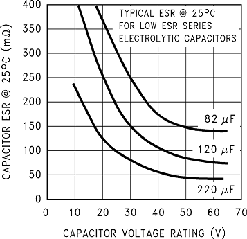 Figure 24. Capacitor ESR vs Capacitor Voltage Rating (Typical Low ESR Electrolytic Capacitor)
Table 1. Output Capacitor and Feedforward Capacitor Selection Table
| OUTPUT VOLTAGE (V) | THROUGH-HOLE OUTPUT CAPACITOR | SURFACE-MOUNT OUTPUT CAPACITOR | ||||
|---|---|---|---|---|---|---|
| PANASONIC HFQ SERIES (µF/V) | NICHICON PL SERIES (µF/V) | FEEDFORWARD CAPACITOR | AVX TPS SERIES (µF/V) | SPRAGUE 595D SERIES (µF/V) | FEEDFORWARD CAPACITOR | |
| 9 | 180/25 | 180/25 | 1.5 nF | 100/16 | 180/16 | 1.5 nF |
| 12 | 120/25 | 120/25 | 1.5 nF | 68/20 | 120/20 | 1.5 nF |
| 15 | 120/25 | 120/25 | 1.5 nF | 68/20 | 100/20 | 1.5 nF |
| 24 | 82/35 | 82/35 | 1 nF | 33/25 | 33/35 | 220 pF |
| 28 | 82/50 | 82/50 | 1 nF | 10/35 | 33/35 | 220 pF |
9.1.4 Catch Diode
Buck regulators require a diode to provide a return path for the inductor current when the switch turns off. This must be a fast diode and must be placed close to the LM2595 using short leads and short printed circuit traces.
Because of their very fast switching speed and low forward voltage drop, Schottky diodes provide the best performance, especially in low output voltage applications (5 V and lower). Ultra-fast recovery, or high-efficiency rectifiers are also a good choice, but some types with an abrupt turnoff characteristic may cause instability or EMI problems. Ultra-fast recovery diodes typically have reverse recovery times of 50 ns or less. Rectifiers such as the 1N5400 series are much too slow and must not be used.
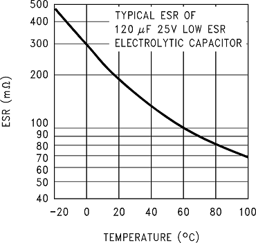 Figure 25. Capacitor ESR Change vs Temperature
Table 2. Diode Selection Table
| VR | 1-A DIODES | 3-A DIODES | ||||||
|---|---|---|---|---|---|---|---|---|
| SURFACE MOUNT | THROUGH HOLE | SURFACE MOUNT | THROUGH HOLE | |||||
| SCHOTTKY | ULTRA FAST RECOVERY | SCHOTTKY | ULTRA FAST RECOVERY | SCHOTTKY | ULTRA FAST RECOVERY | SCHOTTKY | ULTRA FAST RECOVERY | |
| 20 V | SK12 | All of these diodes are rated to at least 50 V |
1N5817 | All of these diodes are rated to at least 50 V |
All of these diodes are rated to at least 50 V |
1N5820 | All of these diodes are rated to at least 50 V |
|
| SR102 | SK32 | SR302 | ||||||
| MBR320 | ||||||||
| 30 V | SK13 | 1N5818 | 1N5821 | |||||
| MBRS130 | SR103 | SK33 | MBR330 | |||||
| 11DQ03 | 31DQ03 | |||||||
| SK14 | 1N5822 | |||||||
| 40 V | MBRS140 | 1N5819 | SK34 | SR304 | ||||
| 10BQ040 | SR104 | MBRS340 | MBR340 | |||||
| 10MQ040 | MURS120 | 11DQ04 | MUR120 | 30WQ04 | MURS320 | 31DQ04 | MUR320 | |
| 50 V | MBRS160 | 10BF10 | SR105 | SK35 | 30WF10 | SR305 | 30WF10 | |
| or | 10BQ050 | MBR150 | MBR360 | MBR350 | ||||
| More | 10MQ060 | 11DQ05 | 30WQ05 | 31DQ05 | ||||
9.1.5 Inductor Selection
All switching regulators have two basic modes of operation: continuous and discontinuous. The difference between the two types relates to the inductor current, whether it is flowing continuously, or if it drops to zero for a period of time in the normal switching cycle. Each mode has distinctively different operating characteristics, which can affect the regulators performance and requirements. Most switcher designs will operate in the discontinuous mode when the load current is low.
The LM2595 (or any of the Simple Switcher family) can be used for both continuous or discontinuous modes of operation.
In many cases the preferred mode of operation is the continuous mode. This mode offers greater output power, lower peak switch, inductor and diode currents, and can have lower output ripple voltage. However, the continuous mode requires larger inductor values to keep the inductor current flowing continuously, especially at low output load currents and/or high input voltages.
To simplify the inductor selection process, an inductor selection guide (nomograph) was designed (see Figure 27 through Figure 30). This guide assumes that the regulator is operating in the continuous mode, and selects an inductor that will allow a peak-to-peak inductor ripple current to be a certain percentage of the maximum design load current. This peak-to-peak inductor ripple current percentage is not fixed, but is allowed to change as different design load currents are selected. (See Figure 26.)
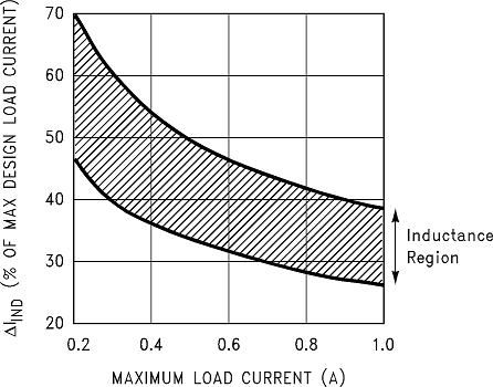 Figure 26. ΔIIND, Peak-to-Peak Inductor Ripple Current
(as a Percentage of the Load Current) vs Load Current
By allowing the percentage of inductor ripple current to increase for low load currents, the inductor value and size can be kept relatively low.
When operating in the continuous mode, the inductor current waveform ranges from a triangular to a sawtooth type of waveform (depending on the input voltage), with the average value of this current waveform equal to the DC output load current.
Inductors are available in different styles such as pot core, toroid, E-core, bobbin core, and so forth, as well as different core materials, such as ferrites and powdered iron. The least expensive, the bobbin, rod or stick core, consists of wire wound on a ferrite bobbin. This type of construction makes for an inexpensive inductor; however, because the magnetic flux is not completely contained within the core, it generates more Electro-Magnetic Interference (EMl). This magnetic flux can induce voltages into nearby printed circuit traces, thus causing problems with both the switching regulator operation and nearby sensitive circuitry, and can give incorrect scope readings because of induced voltages in the scope probe (see Open Core Inductors).
When multiple switching regulators are placed on the same PCB, open core magnetics can cause interference between two or more of the regulator circuits, especially at high currents. A toroid or E-core inductor (closed magnetic structure) must be used in these situations.
The inductors listed in the selection chart include ferrite E-core construction for Schott, ferrite bobbin core for Renco and Coilcraft, and powdered iron toroid for Pulse Engineering.
Exceeding an inductor's maximum current rating may cause the inductor to overheat because of the copper wire losses, or the core may saturate. If the inductor begins to saturate, the inductance decreases rapidly and the inductor begins to look mainly resistive (the DC resistance of the winding). This can cause the switch current to rise very rapidly and force the switch into a cycle-by-cycle current limit, thus reducing the DC output load current. This can also result in overheating of the inductor and/or the LM2595. Different inductor types have different saturation characteristics, and this must be kept in mind when selecting an inductor.
The inductor manufacturer's data sheets include current and energy limits to avoid inductor saturation.
For continuous mode operation, see the inductor selection graphs in Figure 27 through Figure 30
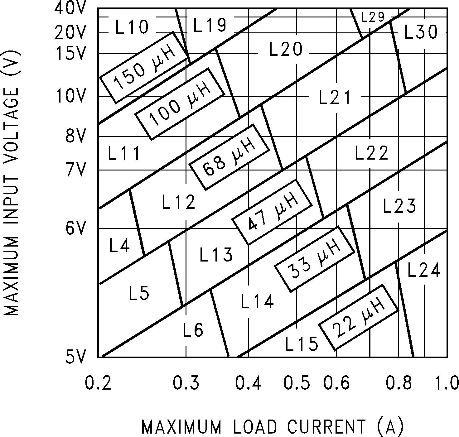 Figure 27. LM2595 3.3-V
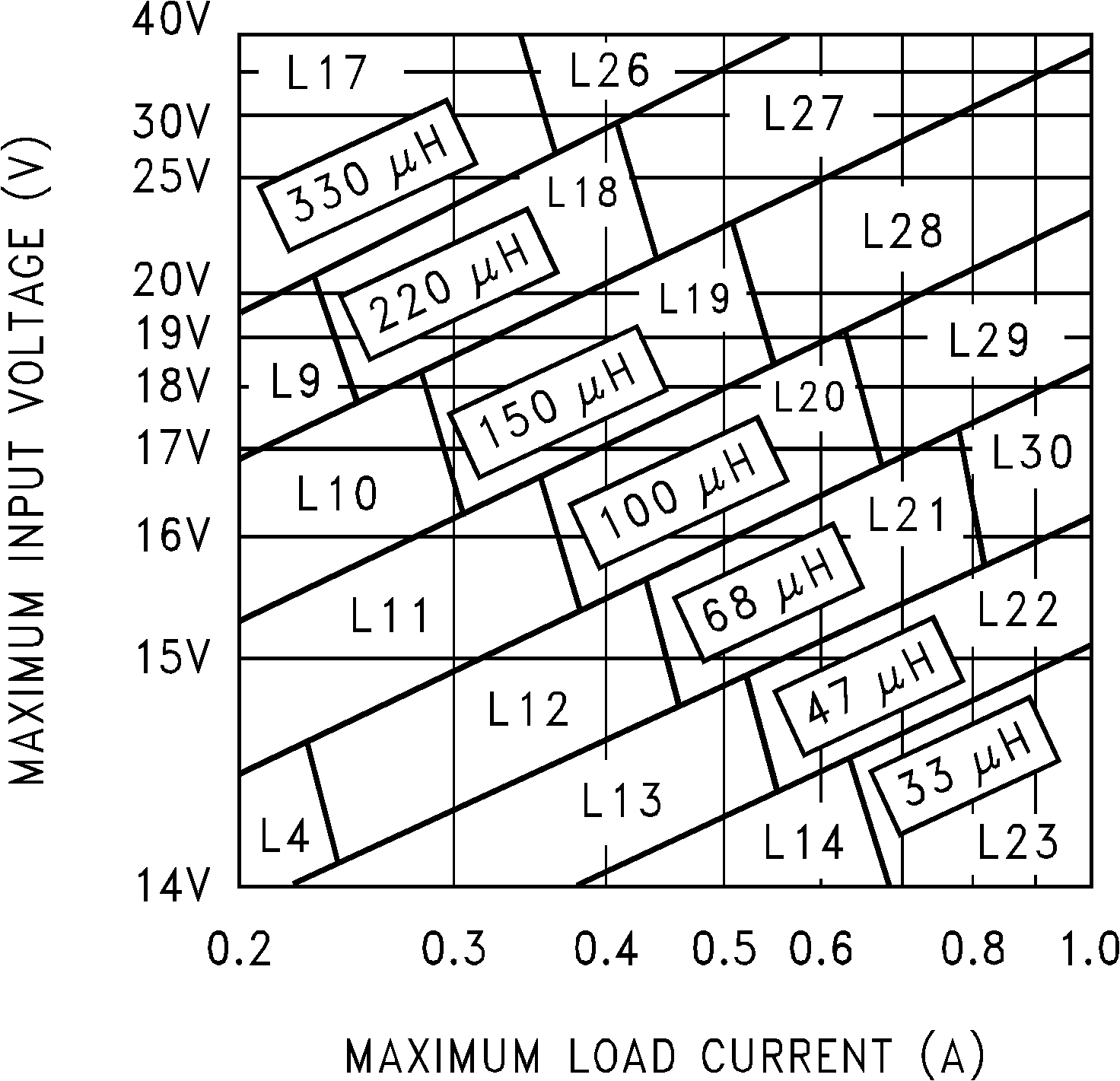 Figure 29. LM2595 12-V
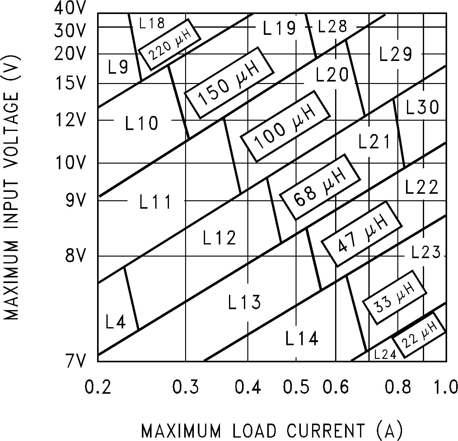 Figure 28. LM2595 5-V
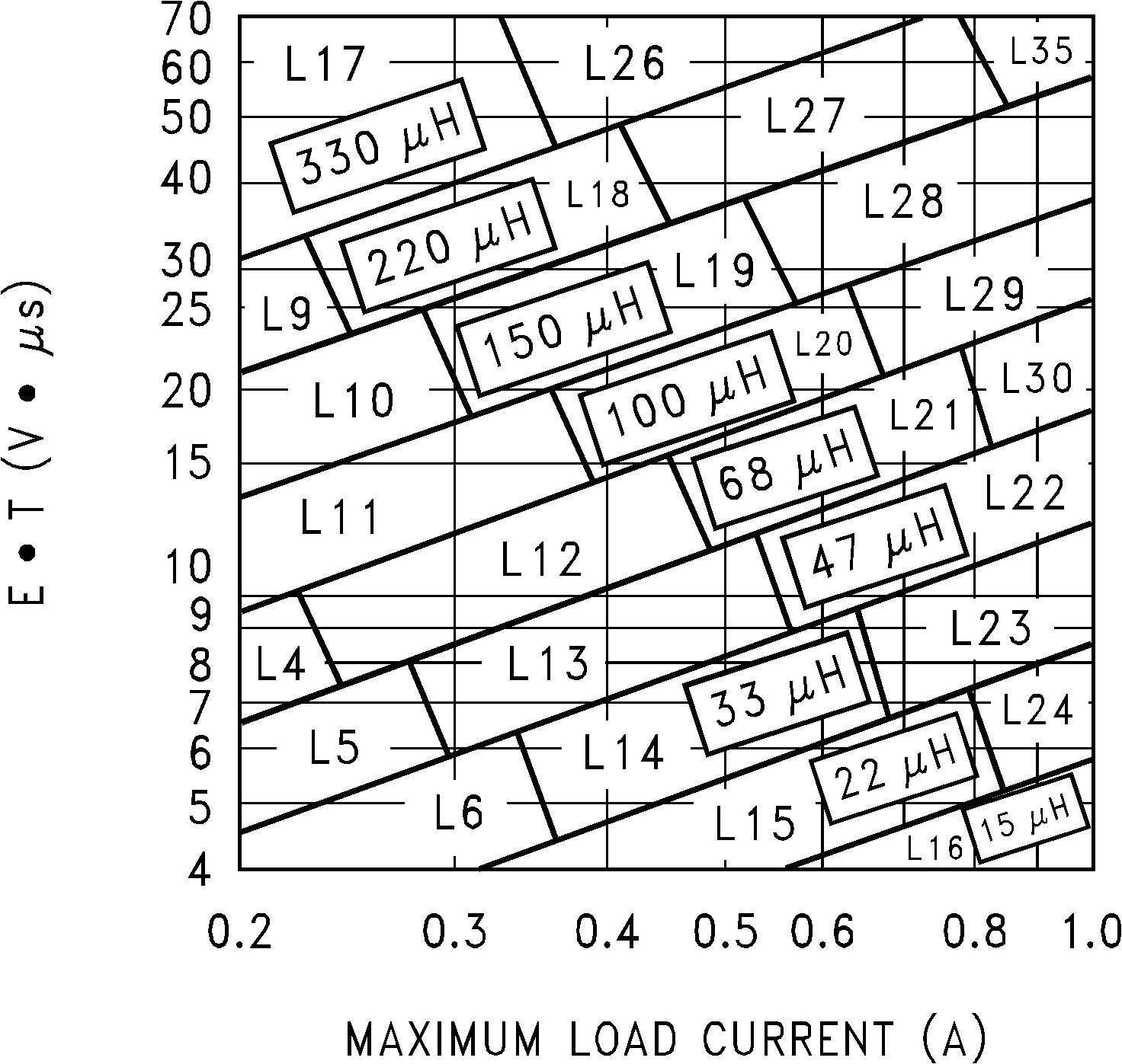 Figure 30. LM2595 Adjustable Voltage
Table 3. Inductor Manufacturer's Part Numbers
| INDUCTANCE (μH) |
CURRENT (A) |
RENCO | PULSE ENGINEERING | COILCRAFT | |||
|---|---|---|---|---|---|---|---|
| THROUGH HOLE | SURFACE MOUNT | THROUGH HOLE | SURFACE MOUNT | SURFACE MOUNT | |||
| L4 | 68 | 0.32 | RL-1284-68-43 | RL1500-68 | PE-53804 | PE-53804-S | DO1608-68 |
| L5 | 47 | 0.37 | RL-1284-47-43 | RL1500-47 | PE-53805 | PE-53805-S | DO1608-473 |
| L6 | 33 | 0.44 | RL-1284-33-43 | RL1500-33 | PE-53806 | PE-53806-S | DO1608-333 |
| L9 | 220 | 0.32 | RL-5470-3 | RL1500-220 | PE-53809 | PE-53809-S | DO3308-224 |
| L10 | 150 | 0.39 | RL-5470-4 | RL1500-150 | PE-53810 | PE-53810-S | DO3308-154 |
| L11 | 100 | 0.48 | RL-5470-5 | RL1500-100 | PE-53811 | PE-53811-S | DO3308-104 |
| L12 | 68 | 0.58 | RL-5470-6 | RL1500-68 | PE-53812 | PE-53812-S | DO3308-683 |
| L13 | 47 | 0.70 | RL-5470-7 | RL1500-47 | PE-53813 | PE-53813-S | DO3308-473 |
| L14 | 33 | 0.83 | RL-1284-33-43 | RL1500-33 | PE-53814 | PE-53814-S | DO3308-333 |
| L15 | 22 | 0.99 | RL-1284-22-43 | RL1500-22 | PE-53815 | PE-53815-S | DO3308-223 |
| L16 | 15 | 1.24 | RL-1284-15-43 | RL1500-15 | PE-53816 | PE-53816-S | DO3308-153 |
| L17 | 330 | 0.42 | RL-5471-1 | RL1500-330 | PE-53817 | PE-53817-S | DO3316-334 |
| L18 | 220 | 0.55 | RL-5471-2 | RL1500-220 | PE-53818 | PE-53818-S | DO3316-224 |
| L19 | 150 | 0.66 | RL-5471-3 | RL1500-150 | PE-53819 | PE-53819-S | DO3316-154 |
| L20 | 100 | 0.82 | RL-5471-4 | RL1500-100 | PE-53820 | PE-53820-S | DO3316-104 |
| L21 | 68 | 0.99 | RL-5471-5 | RL1500-68 | PE-53821 | PE-53821-S | DO3316-683 |
| L22 | 47 | 1.17 | RL-5471-6 | — | PE-53822 | PE-53822-S | DO3316-473 |
| L23 | 33 | 1.40 | RL-5471-7 | — | PE-53823 | PE-53823-S | DO3316-333 |
| L24 | 22 | 1.70 | RL-1283-22-43 | — | PE-53824 | PE-53824-S | DO3316-223 |
| L26 | 330 | 0.80 | RL-5471-1 | — | PE-53826 | PE-53826-S | DO5022P-334 |
| L27 | 220 | 1.00 | RL-5471-2 | — | PE-53827 | PE-53827-S | DO5022P-224 |
| L28 | 150 | 1.20 | RL-5471-3 | — | PE-53828 | PE-53828-S | DO5022P-154 |
| L29 | 100 | 1.47 | RL-5471-4 | — | PE-53829 | PE-53829-S | DO5022P-104 |
| L30 | 68 | 1.78 | RL-5471-5 | — | PE-53830 | PE-53830-S | DO5022P-683 |
| L35 | 47 | 2.15 | RL-5473-1 | — | PE-53935 | PE-53935-S | — |
9.1.6 Output Voltage Ripple and Transients
The output voltage of a switching power supply operating in the continuous mode will contain a sawtooth ripple voltage at the switcher frequency, and may also contain short voltage spikes at the peaks of the sawtooth waveform.
The output ripple voltage is a function of the inductor sawtooth ripple current and the ESR of the output capacitor. A typical output ripple voltage can range from approximately 0.5% to 3% of the output voltage. To obtain low ripple voltage, the ESR of the output capacitor must be low; however, caution must be exercised when using extremely low ESR capacitors because they can affect the loop stability, resulting in oscillation problems. If very low output ripple voltage is required (less than 20 mV), TI recommends a post ripple filter (see Figure 32). The inductance required is typically between 1 μH and 5 μH, with low DC resistance, to maintain good load regulation. A low ESR output filter capacitor is also required to assure good dynamic load response and ripple reduction. The ESR of this capacitor may be as low as desired, because it is out of the regulator feedback loop. Figure 22 shows a typical output ripple voltage, with and without a post ripple filter.
When observing output ripple with a scope, it is essential that a short, low inductance scope probe ground connection be used. Most scope probe manufacturers provide a special probe terminator which is soldered onto the regulator board, preferably at the output capacitor. This provides a very short scope ground, thus eliminating the problems associated with the 3 inch ground lead normally provided with the probe, and provides a much cleaner and more accurate picture of the ripple voltage waveform.
The voltage spikes are caused by the fast switching action of the output switch and the diode, the parasitic inductance of the output filter capacitor, and its associated wiring. To minimize these voltage spikes, the output capacitor must be designed for switching regulator applications, and the lead lengths must be kept very short. Wiring inductance, stray capacitance, as well as the scope probe used to evaluate these transients, all contribute to the amplitude of these spikes.
When a switching regulator is operating in the continuous mode, the inductor current waveform ranges from a triangular to a sawtooth type of waveform (depending on the input voltage). For a given input and output voltage, the peak-to-peak amplitude of this inductor current waveform remains constant. As the load current increases or decreases, the entire sawtooth current waveform also rises and falls. The average value (or the center) of this current waveform is equal to the DC load current.
If the load current drops to a low enough level, the bottom of the sawtooth current waveform will reach zero, and the switcher will smoothly change from a continuous to a discontinuous mode of operation. Most switcher designs (regardless how large the inductor value is) will be forced to run discontinuous if the output is lightly loaded. This is a perfectly acceptable mode of operation.
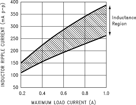 Figure 31. Peak-to-Peak Inductor
Ripple Current vs Load Current
In a switching regulator design, knowing the value of the peak-to-peak inductor ripple current (ΔIIND) can be useful for determining a number of other circuit parameters. Parameters such as, peak inductor or peak switch current, minimum load current before the circuit becomes discontinuous, output ripple voltage and output capacitor ESR can all be calculated from the peak-to-peak ΔIIND. When the inductor nomographs shown in Figure 27 through Figure 30 are used to select an inductor value, the peak-to-peak inductor ripple current can immediately be determined. Figure 31 shows the range of (ΔIIND) that can be expected for different load currents. Figure 31 also shows how the peak-to-peak inductor ripple current (ΔIIND) changes from the lower border to the upper border (for a given load current) within an inductance region. The upper border represents a higher input voltage, while the lower border represents a lower input voltage (see Inductor Selection).
These curves are only correct for continuous mode operation, and only if the inductor selection guides are used to select the inductor value
Consider the following example:
VOUT = 5 V, maximum load current of 800 mA
VIN = 12 V (nominal) varying between 10 V and 14 V
The selection guide in Figure 28 shows that the vertical line for a 0.8-A load current and the horizontal line for the 12-V input voltage intersect approximately midway between the upper and lower borders of the 68-μH inductance region. A 68-μH inductor allows a peak-to-peak inductor current (ΔIIND) to flow as a percentage of the maximum load current. Referring to Figure 31, follow the 0.8-A line approximately midway into the inductance region, and read the peak-to-peak inductor ripple current (ΔIIND) on the left hand axis (approximately 300 mAp-p).
As the input voltage increases to 14 V, it approaches the upper border of the inductance region, and the inductor ripple current increases. Figure 31 shows that for a load current of 0.8 A, the peak-to-peak inductor ripple current (ΔIIND) is 300 mA with 12-V in, and can range from 340 mA at the upper border (14-V in) to 225 mA at the lower border (10-V in).
Once the ΔIIND value is known, the following formulas can be used to calculate additional information about the switching regulator circuit.
- Peak Inductor or peak switch current

- Minimum load current before the circuit becomes discontinuous

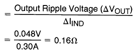
- Output Ripple Voltage = (ΔIIND) × (ESR of COUT)
= 0.30 A × 0.16 Ω = 48 mVp-p - ESR of COUT
9.1.7 Open Core Inductors
Another possible source of increased output ripple voltage or unstable operation is from an open core inductor. Ferrite bobbin or stick inductors have magnetic lines of flux flowing through the air from one end of the bobbin to the other end. These magnetic lines of flux will induce a voltage into any wire or PCB copper trace that comes within the inductor's magnetic field. The strength of the magnetic field, the orientation and location of the PC copper trace to the magnetic field, and the distance between the copper trace and the inductor determine the amount of voltage generated in the copper trace. Another way of looking at this inductive coupling is to consider the PCB copper trace as one turn of a transformer (secondary) with the inductor winding as the primary. Many millivolts can be generated in a copper trace placed near an open core inductor, which can cause stability problems or high output ripple voltage problems.
If unstable operation is seen, and an open core inductor is used, it is possible that the location of the inductor with respect to other PC traces may be the problem. To determine if this is the problem, temporarily raise the inductor away from the board by several inches and then check circuit operation. If the circuit now operates correctly, then the magnetic flux from the open core inductor is causing the problem. Substituting a closed core inductor such as a torroid or E-core will correct the problem, or re-arranging the PC layout may be necessary. Magnetic flux cutting the IC device ground trace, feedback trace, or the positive or negative traces of the output capacitor must be minimized.
Sometimes, placing a trace directly beneath a bobbin inductor will provide good results, provided it is exactly in the center of the inductor (because the induced voltages cancel themselves out). However, if the trace is off center, then problems could arise. If flux problems are present, even the direction of the inductor winding can make a difference in some circuits.
This discussion on open core inductors is not to frighten users, but to alert them on what kind of problems to watch out for. Open core bobbin or stick inductors are an inexpensive, simple way of making a compact, efficient inductor, and they are used by the millions in many different applications.
9.2 Typical Applications
9.2.1 Series Buck Regulator (Fixed Output)
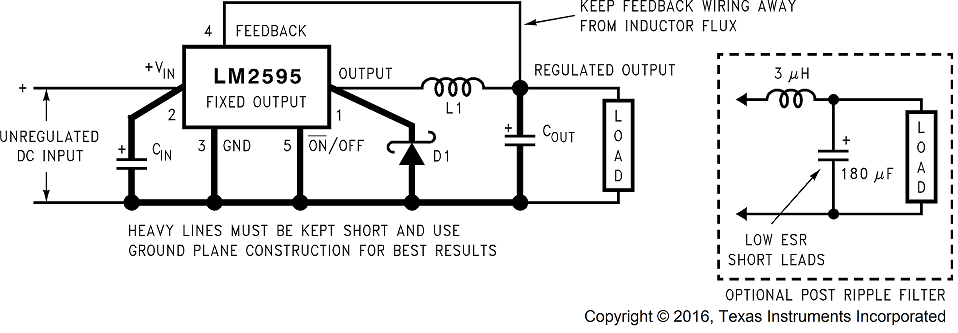
COUT – 120-μF, 25-V aluminum electrolytic Nichicon, PL Series
D1 – 3-A, 40-V Schottky rectifier, 1N5822
L1 – 100-μH, L29
9.2.1.1 Design Requirements
Table 4 lists the parameters for this design example.
Table 4. Example Parameters
| PARAMETER | EXAMPLE VALUE |
|---|---|
| Regulated output voltage (3.3 V, 5 V or 12 V), VOUT | 5 V |
| Maximum DC input voltage, VIN(max) | 12 V |
| Maximum load current, ILOAD(max) | 1 A |
9.2.1.2 Detailed Design Procedure
9.2.1.2.1 Inductor Selection (L1)
- Select the correct inductor value selection guide from Figure 27, Figure 28, or Figure 29 (output voltages of 3.3 V, 5 V, or 12 V respectively).
- From the inductor value selection guide, identify the inductance region intersected by the maximum input voltage line and the maximum load current line. Each region is identified by an inductance value and an inductor code (LXX).
- Select an appropriate inductor from the manufacturer's part numbers listed in Table 3.
Use the inductor selection guide for the 5-V version shown in Figure 28.
From the inductor value selection guide shown in Figure 28, the inductance region intersected by the 12-V horizontal line and the 1-A vertical line is 68 μH, and the inductor code is L30.
The inductance value required is 68 μH. See row L30 of Table 3 and choose an inductor part number from any of the manufactures (in most instance, both through-hole and surface-mount inductors are available).
9.2.1.2.2 Output Capacitor Selection (COUT)
- In the majority of applications, low ESR (Equivalent Series Resistance) electrolytic capacitors between 47 μF and 330 μF and low ESR solid tantalum capacitors between 56 μF and 270 μF provide the best results. This capacitor must be placed close to the IC using short capacitor leads and short copper traces. Do not use capacitors larger than 330 μF.
- To simplify the capacitor selection procedure, see Table 5 for quick design component selection. This table contains different input voltages, output voltages, and load currents, and lists various inductors and output capacitors that will provide the best design solutions.
- 220-μF, 25-V Panasonic HFQ Series
- 220-μF, 25-V Nichicon PL Series
- The capacitor voltage rating for electrolytic capacitors must be at least 1.5 times greater than the output voltage, and often much higher voltage ratings are required to satisfy the low ESR requirements for low output ripple voltage.
From Table 5, place the 5-V output voltage section. In the load current column, choose the load current line that is closest to the current required in the application; for this example, use the 1-A line. In the maximum input voltage column, select the line that covers the input voltage required in the application; in this example, use the 15-V line. The rest of this line shows the recommended inductors and capacitors that will provide the best overall performance.
The capacitor list contains both through-hole electrolytic and surface-mount tantalum capacitors from four different capacitor manufacturers. TI recommends using both the manufacturers and the manufacturer's series listed in Table 5.
In this example, aluminum electrolytic capacitors from several different manufacturers are available with the range of ESR numbers required:
For a 5-V output, a capacitor voltage rating at least 7.5 V or more is required. But, in this example, even a low ESR, switching grade, 220-μF, 10-V aluminum electrolytic capacitor would exhibit approximately 225 mΩ of ESR (see Figure 24 for the ESR versus voltage rating). This amount of ESR would result in relatively high output ripple voltage. To reduce the ripple to 1% of the output voltage, or less, a capacitor with a higher voltage rating (lower ESR) must be selected. A 16-V or 25-V capacitor will reduce the ripple voltage by approximately half.
9.2.1.2.3 Catch Diode Selection (D1)
- The catch diode current rating must be at least 1.3 times greater than the maximum load current. Also, if the power supply design must withstand a continuous output short, the diode must have a current rating equal to the maximum current limit of the LM2595. The most stressful condition for this diode is an overload or shorted output condition.
- The reverse voltage rating of the diode must be at least 1.25 times the maximum input voltage.
- This diode must be fast (short reverse recovery time) and must be placed close to the LM2595 using short leads and short printed circuit traces. Because of their fast switching speed and low forward voltage drop, Schottky diodes provide the best performance and efficiency, and must be the first choice, especially in low output voltage applications. Ultra-fast recovery, or high-efficiency rectifiers also provide good results. Ultra-fast recovery diodes typically have reverse recovery times of 50 ns or less. Rectifiers such as the 1N5400 series must not be used because they are too slow.
See Table 2. In this example, a 3-A, 20-V, 1N5820 Schottky diode will provide the best performance, and will not be overstressed even for a shorted output.
9.2.1.2.4 Input Capacitor (CIN)
A low ESR aluminum or tantalum bypass capacitor is required between the input pin and ground pin to prevent large voltage transients from appearing at the input. This capacitor must be placed close to the IC using short leads. In addition, the RMS current rating of the input capacitor must be selected to be at least ½ the DC load current. The capacitor manufacturer's data sheet must be checked to assure that this current rating is not exceeded. Figure 23 shows typical RMS current ratings for several different aluminum electrolytic capacitor values.
The important parameters for the input capacitor are the input voltage rating and the RMS current rating. With a nominal input voltage of 12 V, an aluminum electrolytic capacitor with a voltage rating greater than 18 V
(1.5 × VIN) is necessary. The next higher capacitor voltage rating is 25 V.
For an aluminum electrolytic, the capacitor voltage rating must be approximately 1.5 times the maximum input voltage. Exercise caution if solid tantalum capacitors are used (see Input Capacitor (CIN) on input capacitor). The tantalum capacitor voltage rating must be 2 times the maximum input voltage and TI recommends that they be surge current tested by the manufacturer.
The RMS current rating requirement for the input capacitor in a buck regulator is approximately ½ the DC load current. In this example, with a 1-A load, a capacitor with a RMS current rating of at least 500 mA is required. Figure 23 can be used to select an appropriate input capacitor. From the curves, place the 25-V line and note which capacitor values have RMS current ratings greater than 500 mA. Either a 180-μF or 220-μF, 25-V capacitor could be used.
Use caution when using ceramic capacitors for input bypassing, because it may cause severe ringing at the VIN pin.
For a through-hole design, a 220-μF, 25-V electrolytic capacitor (Panasonic HFQ series or Nichicon PL series or equivalent) would be adequate. Other types or other manufacturers' capacitors can be used provided the RMS ripple current ratings are adequate.
For surface-mount designs, solid tantalum capacitors can be used, but exercise caution with regard to the capacitor surge current rating (see Input Capacitor (CIN) on input capacitors). The TPS series available from AVX, and the 593D series from Sprague are both surge current tested.
Table 5. LM2595 Fixed Voltage Quick Design Component Selection Table
| CONDITIONS | INDUCTOR | OUTPUT CAPACITOR | ||||||
|---|---|---|---|---|---|---|---|---|
| THROUGH-HOLE ELECTROLYTIC | SURFACE-MOUNT TANTALUM | |||||||
| OUTPUT VOLTAGE (V) | LOAD CURRENT (A) | MAX INPUT VOLTAGE (V) | INDUCTANCE (μH) | INDUCTOR (#) | PANASONIC HFQ SERIES (μF/V) | NICHICON PL SERIES (μF/V) | AVX TPS SERIES (μF/V) | SPRAGUE 595D SERIES (μF/V) |
| 3.3 | 1 | 5 | 22 | L24 | 330/16 | 330/16 | 220/10 | 330/10 |
| 7 | 33 | L23 | 270/25 | 270/25 | 220/10 | 270/10 | ||
| 10 | 47 | L31 | 220/25 | 220/35 | 220/10 | 220/10 | ||
| 40 | 68 | L30 | 180/35 | 220/35 | 220/10 | 180/10 | ||
| 6 | 47 | L13 | 220/25 | 220/16 | 220/10 | 220/10 | ||
| 0.5 | 10 | 68 | L21 | 150/35 | 150/25 | 100/16 | 150/16 | |
| 40 | 100 | L20 | 150/35 | 82/35 | 100/16 | 100/20 | ||
| 5 | 1 | 8 | 33 | L28 | 330/16 | 330/16 | 220/10 | 270/10 |
| 10 | 47 | L31 | 220/25 | 220/25 | 220/10 | 220/10 | ||
| 15 | 68 | L30 | 180/35 | 180/35 | 220/10 | 150/16 | ||
| 40 | 100 | L29 | 180/35 | 120/35 | 100/16 | 120/16 | ||
| 9 | 68 | L21 | 180/16 | 180/16 | 220/10 | 150/16 | ||
| 0.5 | 20 | 150 | L19 | 120/25 | 1200/25 | 100/16 | 100/20 | |
| 40 | 150 | L19 | 100/25 | 100/25 | 68/20 | 68/25 | ||
| 12 | 1 | 15 | 47 | L31 | 220/25 | 220/25 | 68/20 | 120/20 |
| 18 | 68 | L30 | 180/35 | 120/25 | 68/20 | 120/20 | ||
| 30 | 150 | L36 | 82/25 | 82/25 | 68/20 | 100/20 | ||
| 40 | 220 | L35 | 82/25 | 82/25 | 68/20 | 68/25 | ||
| 15 | 68 | L21 | 180/25 | 180/25 | 68/20 | 120/20 | ||
| 0.5 | 20 | 150 | L19 | 82/25 | 82/25 | 68/20 | 100/20 | |
| 40 | 330 | L26 | 56/25 | 56/25 | 68/20 | 68/25 | ||
9.2.1.3 Application Curves
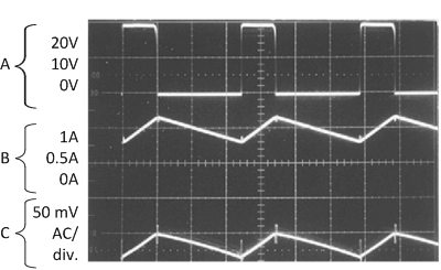
L = 68 μH, COUT = 120 μF, COUT ESR = 100 mΩ
A: Output pin voltage, 10 V/div.
B: Inductor current, 0.5 A/div.
C: Output ripple voltage, 50 mV/div.
Horizontal time base: 2 µs/div.
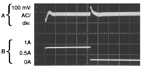
L = 68 μH, COUT = 120 μF, COUT ESR = 100 mΩ
A: Output voltage, 100 mV/div. (AC)
B: 250-mA to 750-mA load pulse
Horizontal time base: 100 µs/div.
9.2.2 Series Buck Regulator (Adjustable Output)
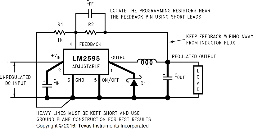
 CIN – 120-μF, 50-V aluminum electrolytic Nichicon, PL Series
COUT – 120-μF, 25-V aluminum electrolytic Nichicon, PL Series
D1 – 3-A, 40-V Schottky rectifier, 1N5822
L1 – 100-μH, L29
R1 – 1-kΩ, 1%
CFF – See Feedforward Capacitor (CFF)
9.2.2.1 Design Requirements
Table 6 lists the parameters for this design example.
Table 6. Example Parameters
| PARAMETER | EXAMPLE VALUE |
|---|---|
| Regulated output voltage, VOUT | 20 V |
| Maximum input voltage, VIN(max) | 28 V |
| Maximum load current, ILOAD(max) | 1 A |
| Switching frequency, F | Fixed at a nominal 150 kHz |
9.2.2.2 Detailed Design Procedure
9.2.2.2.1 Programming Output Voltage
Select the R1 and R2.
Use Equation 1 to select the appropriate resistor values.

Select a value for R1 between 240 Ω and 1.5 kΩ in Equation 2. The lower resistor values minimize noise pickup in the sensitive feedback pin (for the lowest temperature coefficient and the best stability with time, use 1% metal film resistors).

Select R1 to be 1 kΩ, 1%. Solve for R2 in Equation 3.

R2 = 1k (16.26 − 1) = 15.26k, closest 1% value is 15.4 kΩ.
R2 = 15.4 kΩ.
9.2.2.2.2 Inductor Selection (L1)
- Calculate the inductor Volt • microsecond constant E • T (V • μs) with Equation 4.
- VSAT = internal switch saturation voltage = 1 V
- and VD = diode forward voltage drop = 0.5 V
- Use the E • T value from the previous formula and match it with the E • T number on the vertical axis of the Inductor Value Selection Guide shown in Figure 30.
- On the horizontal axis, select the maximum load current.
- Identify the inductance region intersected by the E • T value and the Maximum Load Current value. Each region is identified by an inductance value and an inductor code (LXX).
- Select an appropriate inductor from the manufacturers' part numbers listed in Table 3.

where
Calculate the inductor Volt • microsecond constant (E • T) with Equation 5.

E • T = 34.8 (V • μs)
ILOAD(max) = 1 A
From the inductor value selection guide shown in Figure 30, the inductance region intersected by the 35 (V • μs) horizontal line and the 1-A vertical line is 100 μH, and the inductor code is L29.
From the table in Table 3, place line L29, and select an inductor part number from the list of manufacturers' part numbers.
9.2.2.2.3 Output Capacitor Selection (COUT)
- In the majority of applications, low ESR electrolytic or solid tantalum capacitors between 47 μF and 330 μF provide the best results. This capacitor must be placed close to the IC using short capacitor leads and short copper traces. Do not use capacitors larger than 330 μF. See section on COUT in Output Capacitor Selection (COUT).
- To simplify the capacitor selection procedure, refer to the quick design table shown in Table 7. This table contains different output voltages, and lists various output capacitors that will provide the best design solutions.
- 82-μF, 35-V Panasonic HFQ Series
- 82-μF, 35-V Nichicon PL Series
- The capacitor voltage rating must be at least 1.5 times greater than the output voltage, and often much higher voltage ratings are required to satisfy the low ESR requirements needed for low output ripple voltage.
From the quick design table shown in Table 7, place the output voltage column. From that column, place the output voltage closest to the output voltage in the application. In this example, select the 24-V line. Under the output capacitor section, select a capacitor from the list of through-hole electrolytic or surface-mount tantalum types from four different capacitor manufacturers. TI recommends using both the manufacturers and the manufacturers' series listed in the table.
In this example, through-hole aluminum electrolytic capacitors from several different manufacturers are available:
For a 20-V output, a capacitor rating of at least 30 V or more is required. In this example, either a 35-V or 50-V capacitor would work. A 35-V rating was chosen, although a 50-V rating could also be used if a lower output ripple voltage is required.
Other manufacturers or other types of capacitors may also be used, provided the capacitor specifications (especially the 100-kHz ESR) closely match the types listed in Table 7. Refer to the capacitor manufacturers' data sheet for this information.
9.2.2.2.4 Feedforward Capacitor (CFF)
For output voltages greater than approximately 10 V, an additional capacitor is required. The compensation capacitor is typically between 50 pF and 10 nF, and is wired in parallel with the output voltage setting resistor, R2. It provides additional stability for high output voltages, low input or output voltages, or very low ESR output capacitors, such as solid tantalum capacitors. Use Equation 6 to calculate CFF.

This capacitor type can be ceramic, plastic, silver mica, and so forth (because of the unstable characteristics of ceramic capacitors made with Z5U material, they are not recommended).
The table shown in Table 7 contains feedforward capacitor values for various output voltages. In this example, a 1-nF capacitor is required.
9.2.2.2.5 Catch Diode Selection (D1)
- The catch diode current rating must be at least 1.3 times greater than the maximum load current. Also, if the power supply design must withstand a continuous output short, the diode must have a current rating equal to the maximum current limit of the LM2595. The most stressful condition for this diode is an overload or shorted output condition. See Table 2.
- The reverse voltage rating of the diode must be at least 1.25 times the maximum input voltage. Schottky diodes provide the best performance, and in this example a 3-A, 40-V, 1N5822 Schottky diode is a good choice.
- This diode must be fast (short reverse recovery time) and must be placed close to the LM2595 using short leads and short printed circuit traces. Because of their fast switching speed and low forward voltage drop, Schottky diodes provide the best performance and efficiency, and must be the first choice, especially in low output voltage applications. Ultra-fast recovery or high-efficiency rectifiers are also good choices, but some types with an abrupt turnoff characteristic may cause instability or EMl problems. Ultra-fast recovery diodes typically have reverse recovery times of 50 ns or less. Rectifiers such as the 1N4001 series must not be used because they are too slow. The 3-A diode rating is more than adequate and will not be overstressed even for a shorted output.
9.2.2.2.6 Input Capacitor (CIN)
A low ESR aluminum or tantalum bypass capacitor is required between the input pin and ground to prevent large voltage transients from appearing at the input. In addition, the RMS current rating of the input capacitor must be selected to be at least ½ the DC load current. The capacitor manufacturer's data sheet must be checked to assure that this current rating is not exceeded. Figure 23 shows typical RMS current ratings for several different aluminum electrolytic capacitor values.
The important parameters for the input capacitor are the input voltage rating and the RMS current rating. With a nominal input voltage of 28 V, an aluminum electrolytic aluminum electrolytic capacitor with a voltage rating greater than 42 V (1.5 × VIN) is required. Because the next higher capacitor voltage rating is 50 V, a 50-V capacitor must be used. The capacitor voltage rating of (1.5 × VIN) is a conservative guideline, and can be modified somewhat if desired.
This capacitor must be placed close to the IC using short leads and the voltage rating must be approximately 1.5 times the maximum input voltage.
The RMS current rating requirement for the input capacitor of a buck regulator is approximately ½ the DC load current. In this example, with a 1-A load, a capacitor with a RMS current rating of at least 500 mA is required.
Figure 23 can be used to select an appropriate input capacitor. From the curves, place the 50-V line and note which capacitor values have RMS current ratings greater than 500 mA. Either a 100-μF or 120-μF, 50-V capacitor could be used.
If solid tantalum input capacitors are used, TI recommends that they be surge current tested by the manufacturer. See caution when using a high dielectric constant ceramic capacitor for input bypassing, because it may cause severe ringing at the VIN pin.
For a through-hole design, a 120-μF, 50-V electrolytic capacitor (Panasonic HFQ series or Nichicon PL series or equivalent) would be adequate. Other types or other manufacturers' capacitors can be used provided the RMS ripple current ratings are adequate.
For surface-mount designs, solid tantalum capacitors can be used, but caution must be exercised with regard to the capacitor surge current rating (see Input Capacitor (CIN) or input capacitors in this data sheet). The TPS series available from AVX, and the 593D series from Sprague are both surge current tested.
To further simplify the buck regulator design procedure, TI is making available computer design software to be used with the SIMPLE SWITCHER line of switching regulators.
Table 7. Output Capacitor and Feedforward Capacitor Selection Table
| OUTPUT VOLTAGE (V) |
THROUGH-HOLE ELECTROLYTIC OUTPUT CAPACITOR | SURFACE-MOUNT TANTALUM OUTPUT CAPACITOR | ||||
|---|---|---|---|---|---|---|
| PANASONIC HFQ SERIES (μF/V) |
NICHICON PL SERIES (μF/V) |
FEEDFORWARD CAPACITOR |
AVX TPS SERIES (μF/V) |
SPRAGUE 595D SERIES (μF/V) |
FEEDFORWARD CAPACITOR |
|
| 1.2 | 330/50 | 330/50 | 0 | 330/6.3 | 330/6.3 | 0 |
| 4 | 220/25 | 220/25 | 4.7 nF | 220/10 | 220/10 | 4.7 nF |
| 6 | 220/25 | 220/25 | 3.3 nF | 220/10 | 220/10 | 3.3 nF |
| 9 | 180/25 | 180/25 | 1.5 nF | 100/16 | 180/16 | 1.5 nF |
| 12 | 120/25 | 120/25 | 1.5 nF | 68/20 | 120/20 | 1.5 nF |
| 15 | 120/25 | 120/25 | 1.5 nF | 68/20 | 100/20 | 1.5 nF |
| 24 | 82/35 | 82/35 | 1 nF | 33/25 | 33/35 | 220 pF |
| 28 | 82/50 | 82/50 | 1 nF | 10/35 | 33/35 | 220 pF |
9.2.2.3 Application Curves
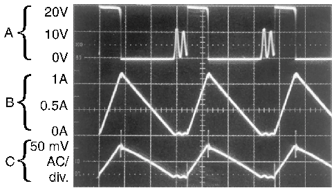
L = 22 μH, COUT = 220 μF, COUT ESR = 50 mΩ
A: Output pin voltage, 10 V/div.
B: Inductor current 0.5 A/div.
C: Output ripple voltage, 50 mV/div.
Horizontal time base: 2 µs/div.
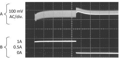
L = 22 μH, COUT = 220 μF, COUT ESR = 50 mΩ
A: Output voltage, 100 mV/div. (AC)
B: 250-mA to 750-mA load pulse
Horizontal time base: 200 µs/div.
for Discontinuous Mode