SNOS965J June   2001  – December 2015 LM2611

PRODUCTION DATA.  

  1. Features
  2. Applications
  3. Description
  4. Revision History
  5. Pin Configuration and Functions
  6. Specifications
    1. 6.1 Absolute Maximum Ratings
    2. 6.2 ESD Ratings
    3. 6.3 Recommended Operating Conditions
    4. 6.4 Thermal Information
    5. 6.5 Electrical Characteristics
  7. Detailed Description
    1. 7.1 Overview
    2. 7.2 Functional Block Diagram
    3. 7.3 Feature Description
      1. 7.3.1 Cuk Converter
      2. 7.3.2 Output and Input Inductor
      3. 7.3.3 Switch Current Limit
      4. 7.3.4 Input Capacitor
      5. 7.3.5 Output Capacitor
      6. 7.3.6 Improving Transient Response and Compensation
    4. 7.4 Device Functional Modes
      1. 7.4.1 Hysteretic Mode
        1. 7.4.1.1 Thermal Shutdown
  8. Application and Implementation
    1. 8.1 Application Information
    2. 8.2 Typical Application
      1. 8.2.1 Cuk Converter With Integrated Switch
        1. 8.2.1.1 Design Requirements
        2. 8.2.1.2 Detailed Design Procedure
        3. 8.2.1.3 Application Curves
      2. 8.2.2 5-V to -5-V Inverting Converter
        1. 8.2.2.1 Design Requirements
        2. 8.2.2.2 Application Curves
      3. 8.2.3 9-V to -5-V Inverting Converter
        1. 8.2.3.1 Design Requirements
        2. 8.2.3.2 Application Curve
      4. 8.2.4 12-V to -5-V Inverting Converter
        1. 8.2.4.1 Design Requirements
        2. 8.2.4.2 Application Curve
      5. 8.2.5 LM2611 Operating With Separate Power and Biasing Supplies
        1. 8.2.5.1 Design Requirements
        2. 8.2.5.2 Detailed Design Procedure
          1. 8.2.5.2.1 Split Supply Operation
      6. 8.2.6 Shutdown and Soft-Start
        1. 8.2.6.1 Design Requirements
        2. 8.2.6.2 Detailed Design Procedure
          1. 8.2.6.2.1 Shutdown and Soft-Start
        3. 8.2.6.3 Application Curves
      7. 8.2.7 High Duty Cycle and Load Current
        1. 8.2.7.1 Design Requirements
        2. 8.2.7.2 Detailed Design Procedure
          1. 8.2.7.2.1 High Duty Cycle and Load Current Operation
  9. Power Supply Recommendations
  10. 10Layout
    1. 10.1 Layout Guidelines
    2. 10.2 Layout Example
  11. 11Device and Documentation Support
    1. 11.1 Community Resources
    2. 11.2 Trademarks
    3. 11.3 Electrostatic Discharge Caution
    4. 11.4 Glossary
  12. 12Mechanical, Packaging, and Orderable Information

Package Options

Mechanical Data (Package|Pins)
Thermal pad, mechanical data (Package|Pins)
Orderable Information

10 Layout

10.1 Layout Guidelines

  • Connection between L1 and SW pin should be kept as short as possible to minimize inductance
  • Connection between CCUK and SW should also be kept short
  • The feedback resistor should be placed close to the NFB pin to minimize the path of the higher impedance feedback node
  • The feedback trace leading from Vout to the output to the feedback resistors should not pass under the switch node between L1 and CCUK and the switch node between CCUK, L2 and D
  • The feedback trace leading from Vout to the output to the feedback resistors should not pass under the inductors L1 and L2
  • A bypass capacitor CBYP of 0.1 µF should be placed close to VIN and GND pin

10.2 Layout Example
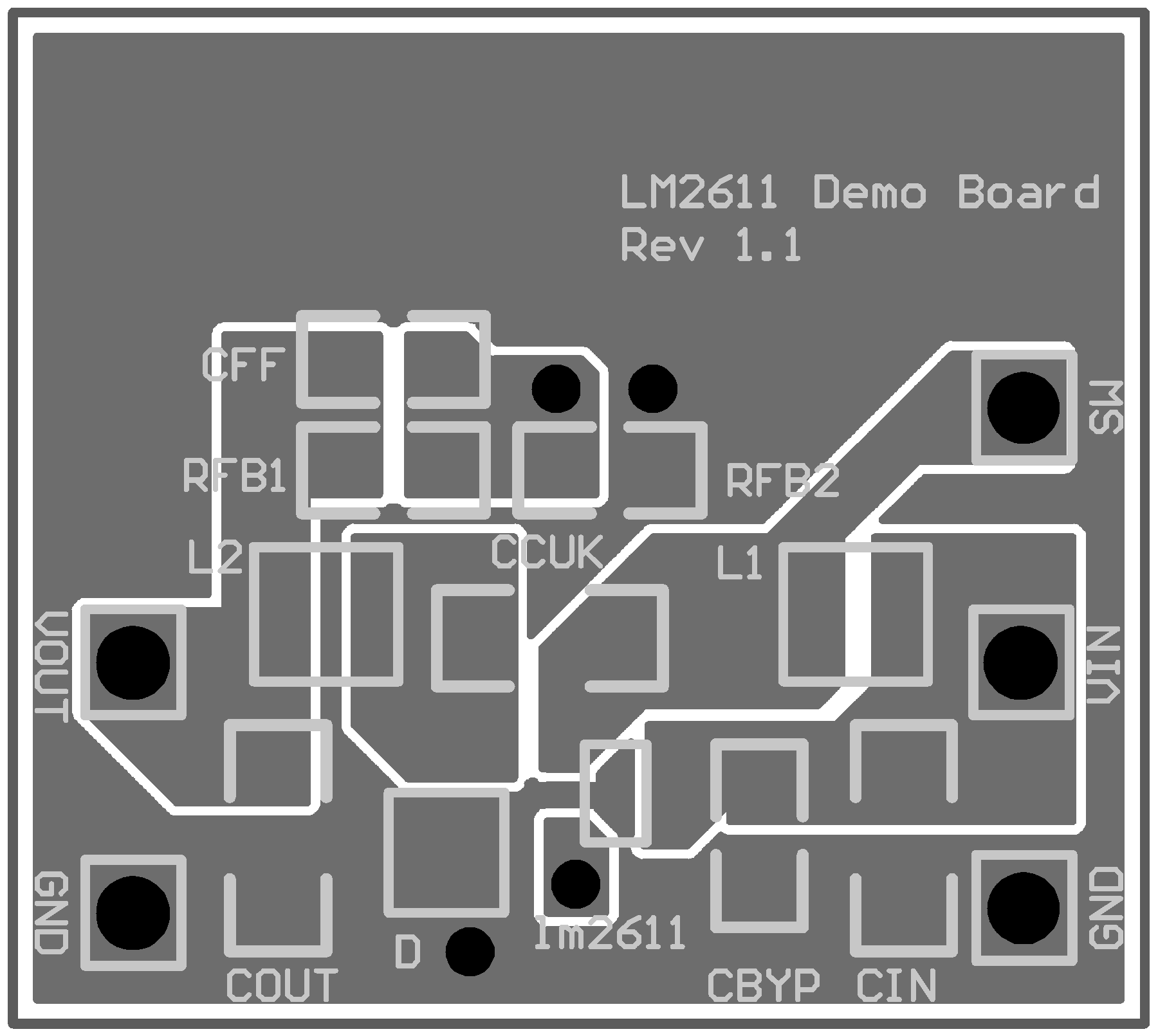
LM2611 layout_example_snos965.png Figure 36. Example Layout Top
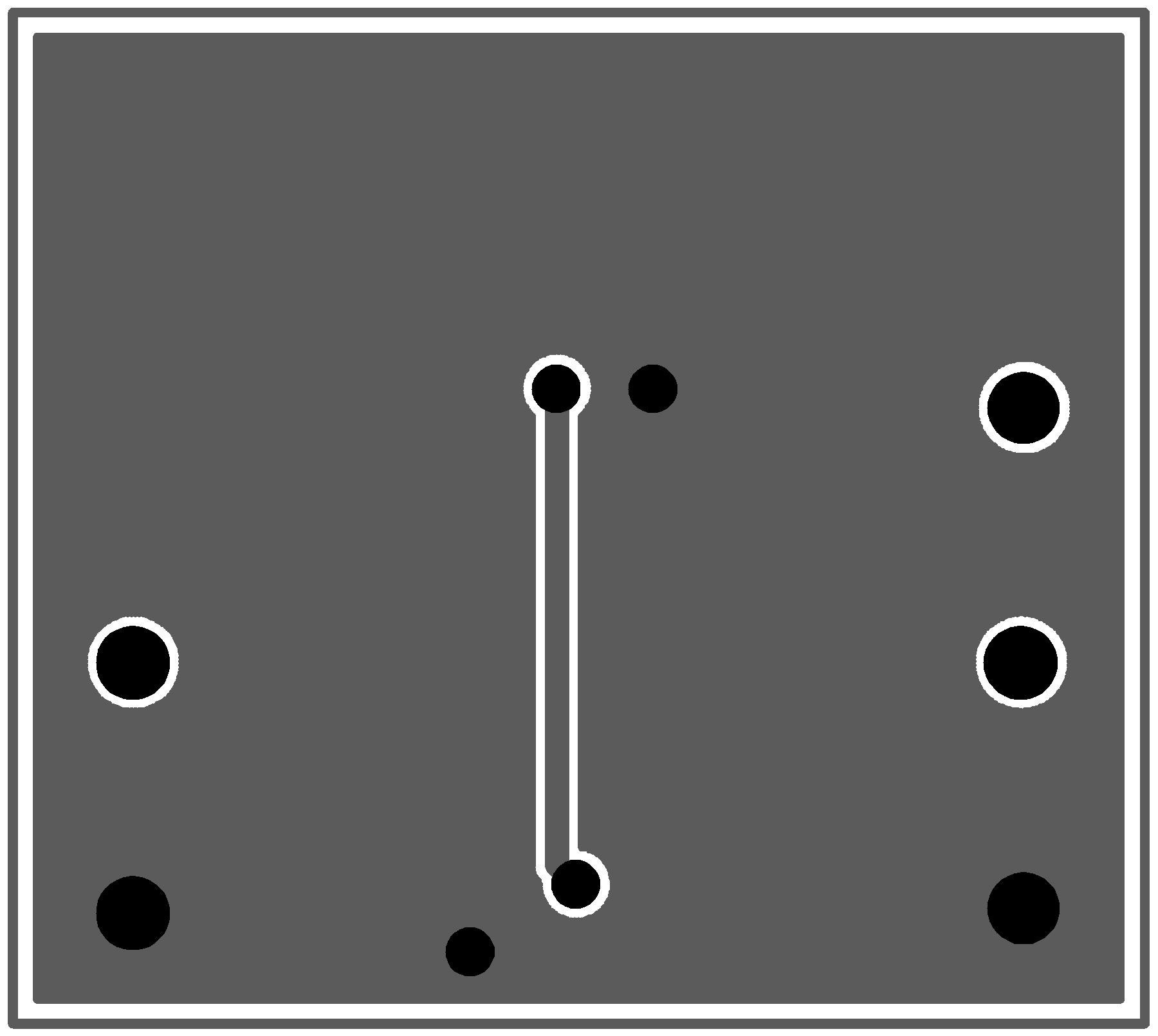
LM2611 20023103.png Figure 37. Example Layout Bottom