SNVSAO5 October 2017 LM2623-Q1
PRODUCTION DATA.
- 1 Features
- 2 Applications
- 3 Description
- 4 Revision History
- 5 Pin Configuration and Functions
- 6 Specifications
- 7 Detailed Description
- 8 Applications and Implementation
- 9 Power Supply Recommendations
- 10Layout
- 11Device And Documentation Support
- 12Mechanical, Packaging, And Orderable Information
Package Options
Mechanical Data (Package|Pins)
- NHL|14
Thermal pad, mechanical data (Package|Pins)
Orderable Information
1 Features
- AEC-Q100 Qualified for Automotive Applications:
- Device Temperature Grade 1: –40°C to 125°C Ambient Operating Temperature
- Device HBM ESD Classification Level 2
- Device CDM ESD Classification Level C4A
- Good Efficiency Over a Very Wide Load Range
- Very Low Output Voltage Ripple
- Up to 2-MHz Switching Frequency
- 0.9-V to 14-V Operating Voltage
- 1.1-V Start-Up Voltage
- 1.24-V to 14-V Adjustable Output Voltage
- 0.17-Ω Internal MOSFET
- Up to 90% Regulator Efficiency
- 80-µA Typical Operating Current (Into VDD Pin of Supply)
- Low Shutdown Current (IQ < 2.5 µA)
- 4-mm × 4-mm Thermally Enhanced WSON Package Option
2 Applications
- Automotive Camera
- Automotive Radar
- Automotive GPS
- Flash Memory Programming
- White-LED Drive
3 Description
The LM2623-Q1 is a high-efficiency, general-purpose, step-up DC-DC switching regulator for automotive systems. The device accepts an input voltage between 0.9 V and 14 V and converts it into a regulated output voltage between 1.24 V and 14 V.
In order to adapt to a number of applications, the LM2623-Q1 allows the designer to program the output voltage, the operating frequency (300 kHz to 2 MHz), and duty cycle (17% to 90%) to optimize performance. The selected values can be fixed or can vary with input voltage or input-to-output voltage ratio. The LM2623-Q1 uses a very simple, on/off regulation mode to produce good efficiency and stable operation over a wide operating range. The device normally regulates by skipping switching cycles when it reaches the regulation limit (pulse frequency modulation (PFM)).
Refer to Non-Linear Effect and Choosing the Correct C3 Capacitor to resolve any design challenges before board design is finalized.
Device Information(1)
| PART NUMBER | PACKAGE | BODY SIZE (NOM) |
|---|---|---|
| LM2623-Q1 | WSON (14) | 4.00 mm × 4.00 mm |
- For all available packages, see the orderable addendum at the end of the data sheet.
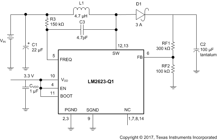
Typical Application
