SNVS005E November 1999 – December 2014 LM2664
PRODUCTION DATA.
- 1 Features
- 2 Applications
- 3 Description
- 4 Revision History
- 5 Pin Configuration and Functions
- 6 Specifications
- 7 Parameter Measurement Information
- 8 Detailed Description
- 9 Application and Implementation
- 10Power Supply Recommendations
- 11Layout
- 12Device and Documentation Support
- 13Mechanical, Packaging, and Orderable Information
Package Options
Mechanical Data (Package|Pins)
- DBV|6
Thermal pad, mechanical data (Package|Pins)
Orderable Information
9 Application and Implementation
NOTE
Information in the following applications sections is not part of the TI component specification, and TI does not warrant its accuracy or completeness. TI’s customers are responsible for determining suitability of components for their purposes. Customers should validate and test their design implementation to confirm system functionality.
9.1 Application Information
The LM2664 CMOS charge-pump voltage converter inverts a positive voltage in the range of 1.8 V to 5.5 V to the corresponding negative voltage of −1.8 V to −5.5 V. The LM2664 uses two low cost capacitors to provide up to 40 mA of output current. The LM2664 operates at 160-kHz oscillator frequency to reduce output resistance and voltage ripple. With an operating current of only 220 µA (operating efficiency greater than 91% with most loads) and 1 µA typical shutdown current, the LM2664 provides ideal performance for battery powered systems.
9.2 Typical Application - Voltage Inverter
 Figure 11. Voltage Inverter
9.2.1 Design Requirements
Example requirements for typical voltage inverter applications:
| DESIGN PARAMETER | EXAMPLE VALUE |
|---|---|
| Input voltage range | 1.8 V to 5.5 V |
| Output current | 0 mA to 40 mA |
| Boost switching frequency | 80 kHz |
9.2.2 Detailed Design Requirements
The main application of LM2664 is to generate a negative supply voltage. The voltage inverter circuit uses only two external capacitors as shown in Voltage Inverter and 5 V to −10 V Converter. The range of the input supply voltage is 1.8 V to 5.5 V.
The output characteristics of this circuit can be approximated by an ideal voltage source in series with a resistance. The voltage source equals −(V+). The output resistance ROUT is a function of the ON resistance of the internal MOSFET switches, the oscillator frequency, the capacitance and equivalent series resistance (ESR) of C1 and C2. Since the switching current charging and discharging C1 is approximately twice as the output current, the effect of the ESR of the pumping capacitor C1 will be multiplied by four in the output resistance. The output capacitor C2 is charging and discharging at a current approximately equal to the output current, therefore, its ESR only counts once in the output resistance. A good approximation of ROUT is:
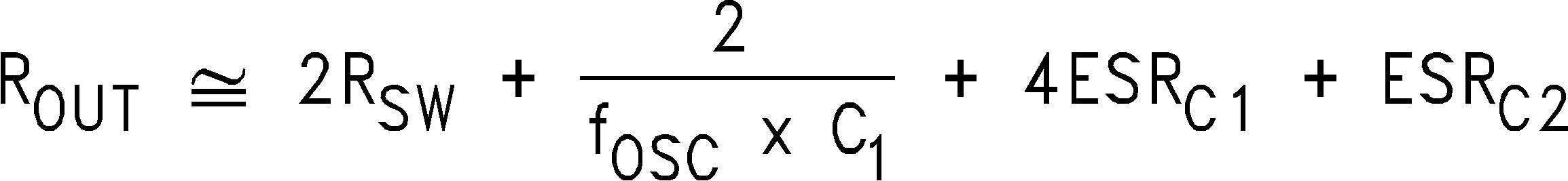
where
- RSW is the sum of the ON resistance of the internal MOSFET switches shown in Figure 10.
High capacitance, low ESR capacitors will reduce the output resistance.
The peak-to-peak output voltage ripple is determined by the oscillator frequency, the capacitance and ESR of the output capacitor C2:
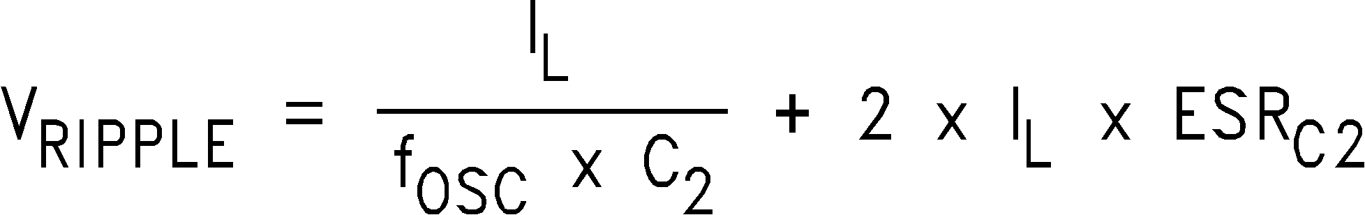
Again, using a low ESR capacitor will result in lower ripple.
9.2.2.1 Paralleling Devices
Any number of LM2664s can be paralleled to reduce the output resistance. Each device must have its own pumping capacitor C1, while only one output capacitor COUT is needed as shown in Figure 12. The composite output resistance is:
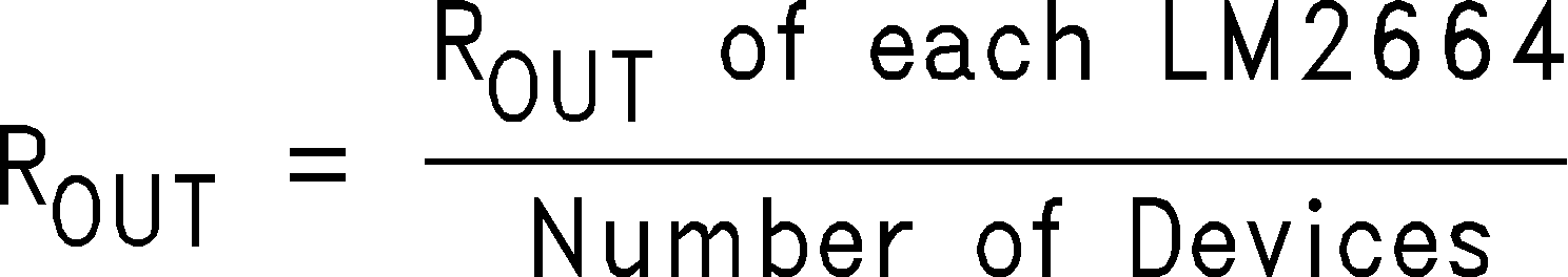
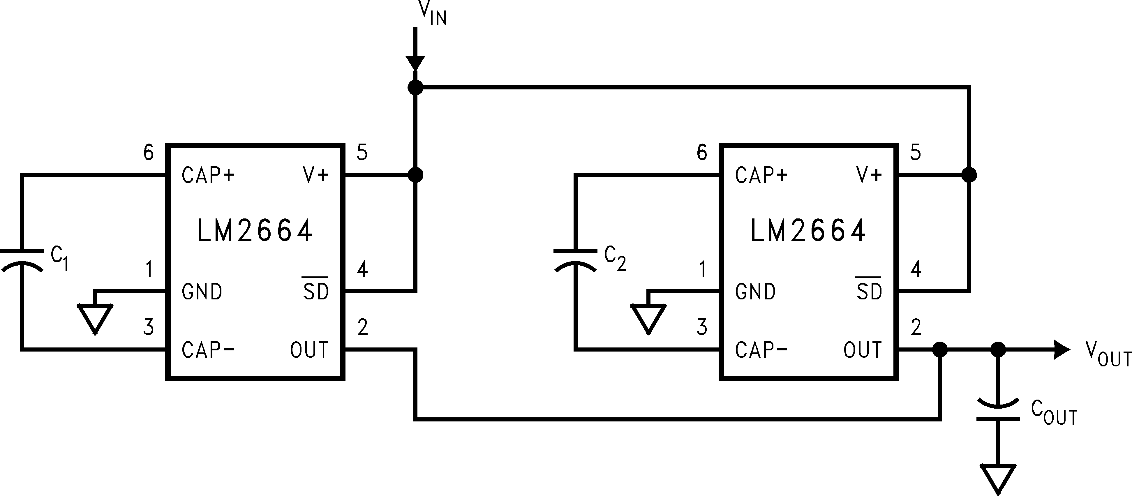 Figure 12. Lowering Output Resistance by Paralleling Devices
9.2.2.2 Cascading Devices
Cascading the LM2664 devices is an easy way to produce a greater negative voltage (a two-stage cascade circuit is shown in Figure 13).
If n is the integer representing the number of devices cascaded, the unloaded output voltage Vout is (-nVin). The effective output resistance is equal to the weighted sum of each individual device:
NOTE
The number of n is practically limited since the increasing of n significantly reduces the efficiency, and increases the output resistance and output voltage ripple.
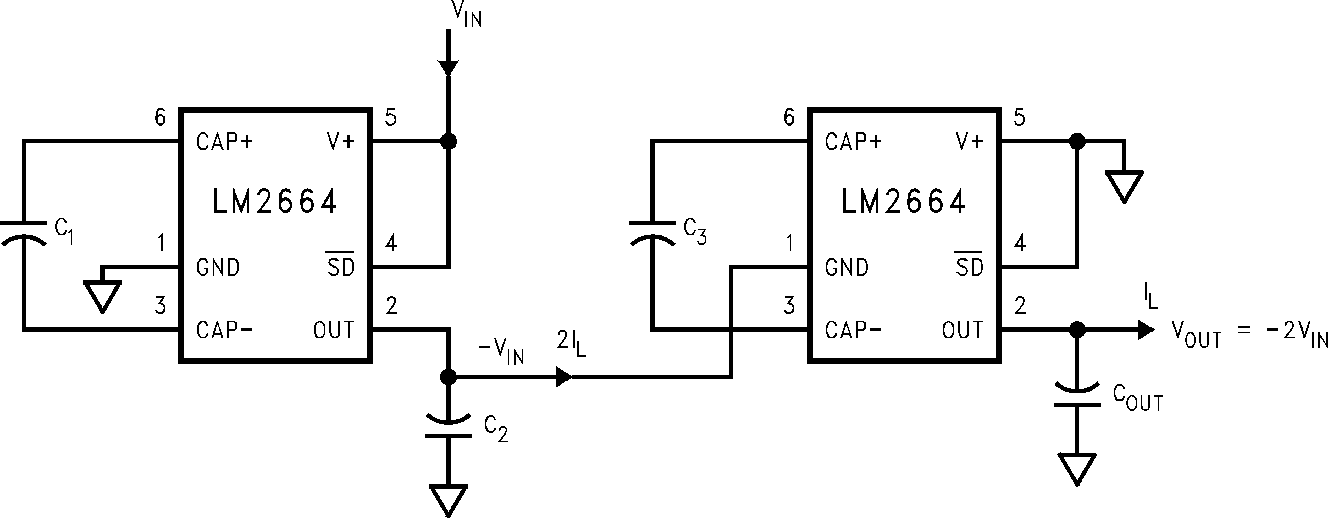 Figure 13. Increasing Output Voltage by Cascading Devices
9.2.2.3 Combined Doubler and Inverter
In Figure 14, the LM2664 is used to provide a positive voltage doubler and a negative voltage converter. Note that the total current drawn from the two outputs should not exceed 50 mA.
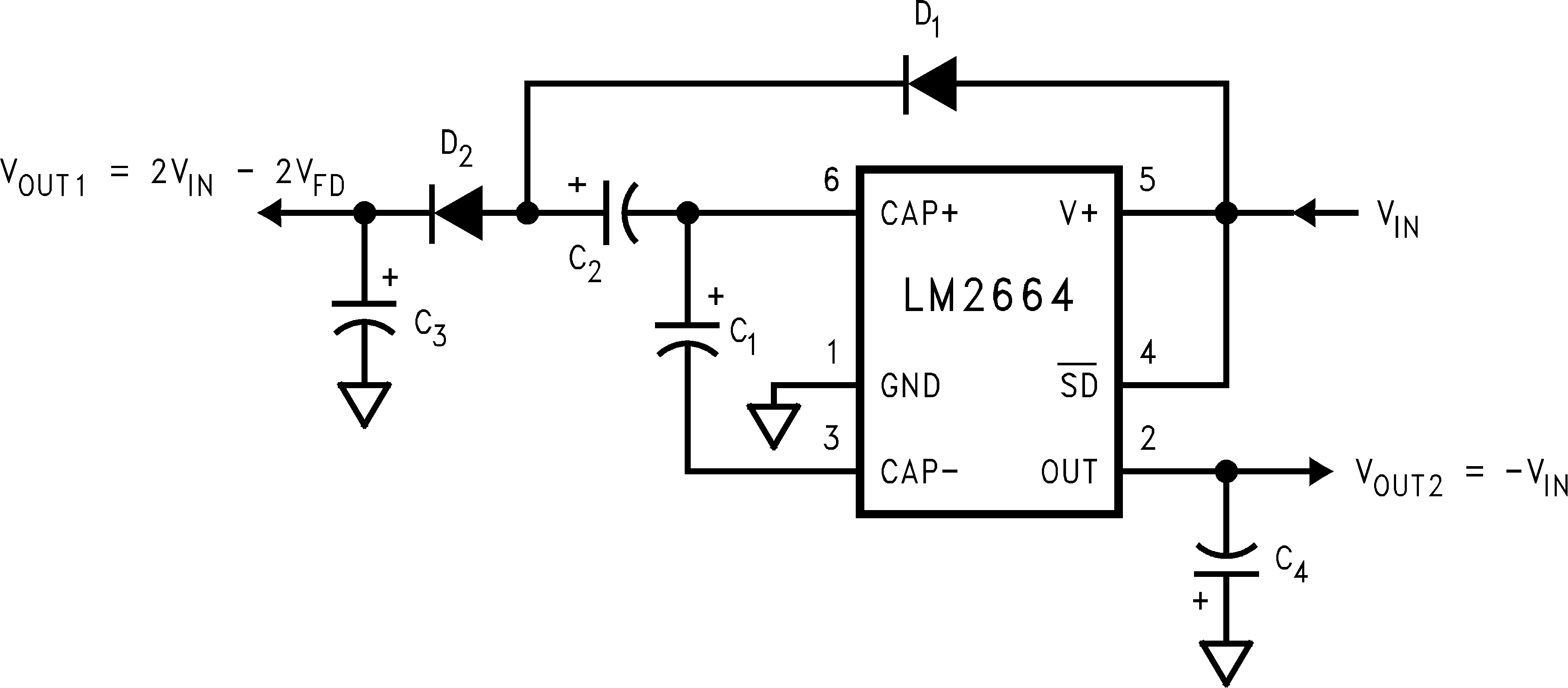 Figure 14. Combined Voltage Doubler and Inverter
9.2.2.4 Regulating VOUT
It is possible to regulate the negative output of the LM2664 by use of a low dropout regulator (such as LP2980). The whole converter is depicted in Figure 15. This converter can give a regulated output from −1.8 V to −5.5 V by choosing the proper resistor ratio:
Note that the following conditions must be satisfied simultaneously for worst case design:
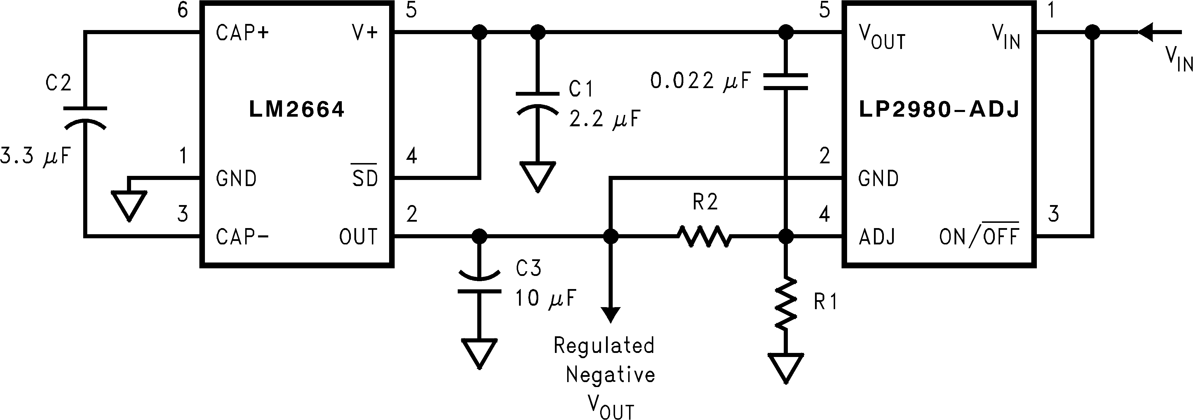 Figure 15. Combining LM2664 with LP2980 to Make a Negative Adjustable Regulator
9.2.2.5 Output Capacitor Selection
As discussed in Detailed Design Requirements, the output resistance and ripple voltage are dependent on the capacitance and ESR values of the external capacitors. The output voltage drop is the load current times the output resistance, and the power efficiency is
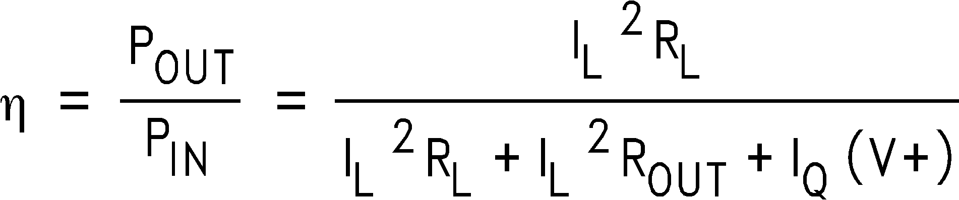
Where IQ(V+) is the quiescent power loss of the IC device, and IL2ROUT is the conversion loss associated with the switch on-resistance, the two external capacitors and their ESRs.
The selection of capacitors is based on the specifications of the dropout voltage (which equals Iout ROUT), the output voltage ripple, and the converter efficiency. Table 1 lists recommendations to maximize efficiency, reduce the output voltage drop and voltage ripple.
Table 1. Low ESR Capacitor Manufacturers
| MANUFACTURER | CAPACITOR TYPE |
|---|---|
| Nichicon Corp. | PL & PF series, through-hole aluminum electrolytic |
| AVX Corp. | TPS series, surface-mount tantalum |
| Sprague | 593D, 594D, 595D series, surface-mount tantalum |
| Sanyo | OS-CON series, through-hole aluminum electrolytic |
| Murata | Ceramic chip capacitors |
| Taiyo Yuden | Ceramic chip capacitors |
| Tokin | Ceramic chip capacitors |
9.2.3 Application Curve
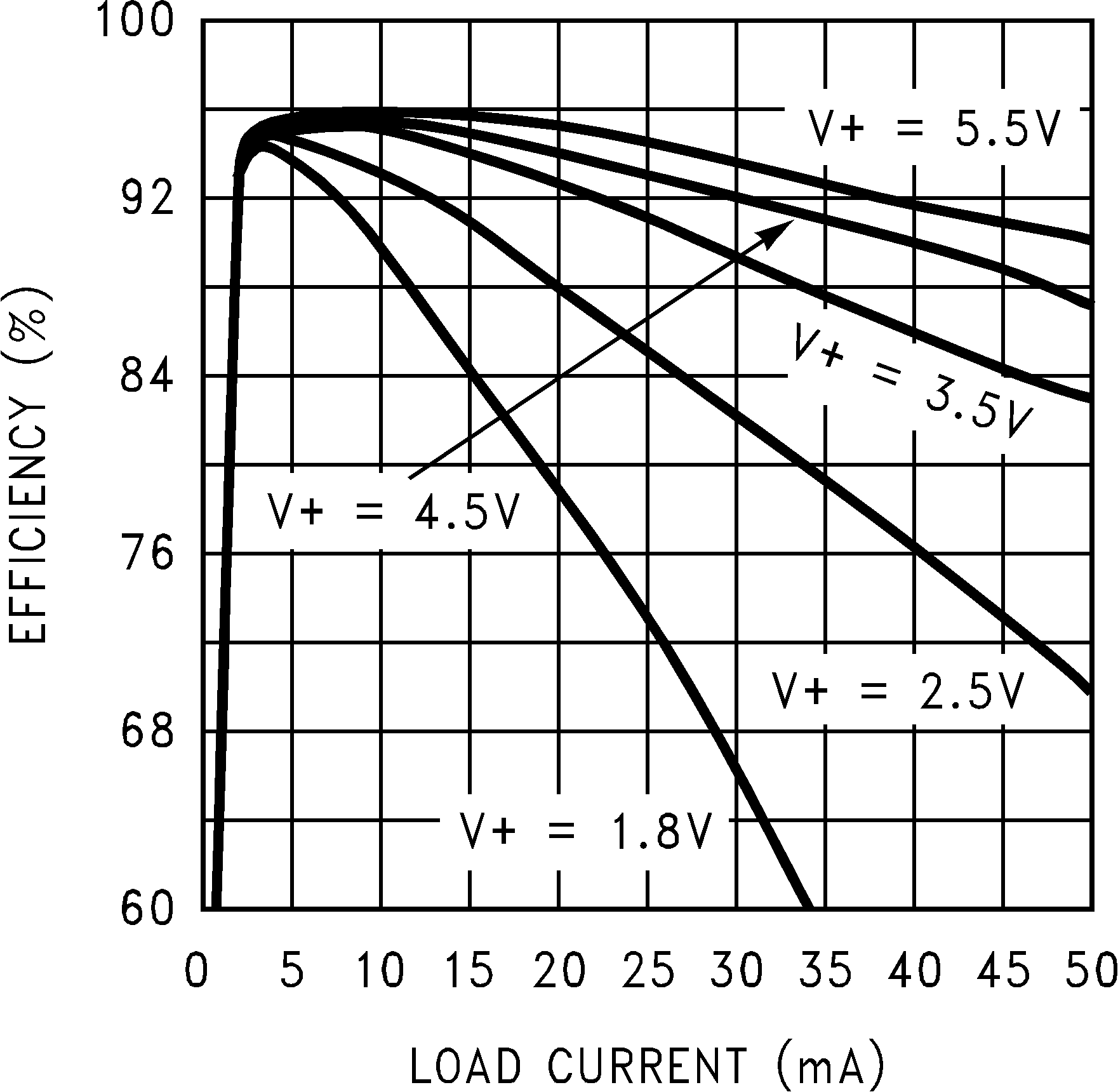 Figure 16. Efficiency vs Load Current