SNVS217G May 2004 – September 2015 LM2731
PRODUCTION DATA.
- 1 Features
- 2 Applications
- 3 Description
- 4 Revision History
- 5 Pin Configuration and Functions
- 6 Specifications
- 7 Detailed Description
-
8 Application and Implementation
- 8.1 Application Information
- 8.2
Typical Application
- 8.2.1 Design Requirements
- 8.2.2
Detailed Design Procedure
- 8.2.2.1 Selecting the External Capacitors
- 8.2.2.2 Selecting the Output Capacitor
- 8.2.2.3 Selecting the Input Capacitor
- 8.2.2.4 Feedforward Compensation
- 8.2.2.5 Selecting Diodes
- 8.2.2.6 Setting the Output Voltage
- 8.2.2.7 Switching Frequency
- 8.2.2.8 Duty Cycle
- 8.2.2.9 Inductance Value
- 8.2.2.10 Maximum Switch Current
- 8.2.2.11 Calculating Load Current
- 8.2.2.12 Design Parameters VSW and ISW
- 8.2.2.13 Inductor Suppliers
- 8.2.3 Application Curves
- 8.3 System Examples
- 9 Power Supply Recommendations
- 10Layout
- 11Device and Documentation Support
- 12Mechanical, Packaging, and Orderable Information
Package Options
Mechanical Data (Package|Pins)
- DBV|5
Thermal pad, mechanical data (Package|Pins)
Orderable Information
7 Detailed Description
7.1 Overview
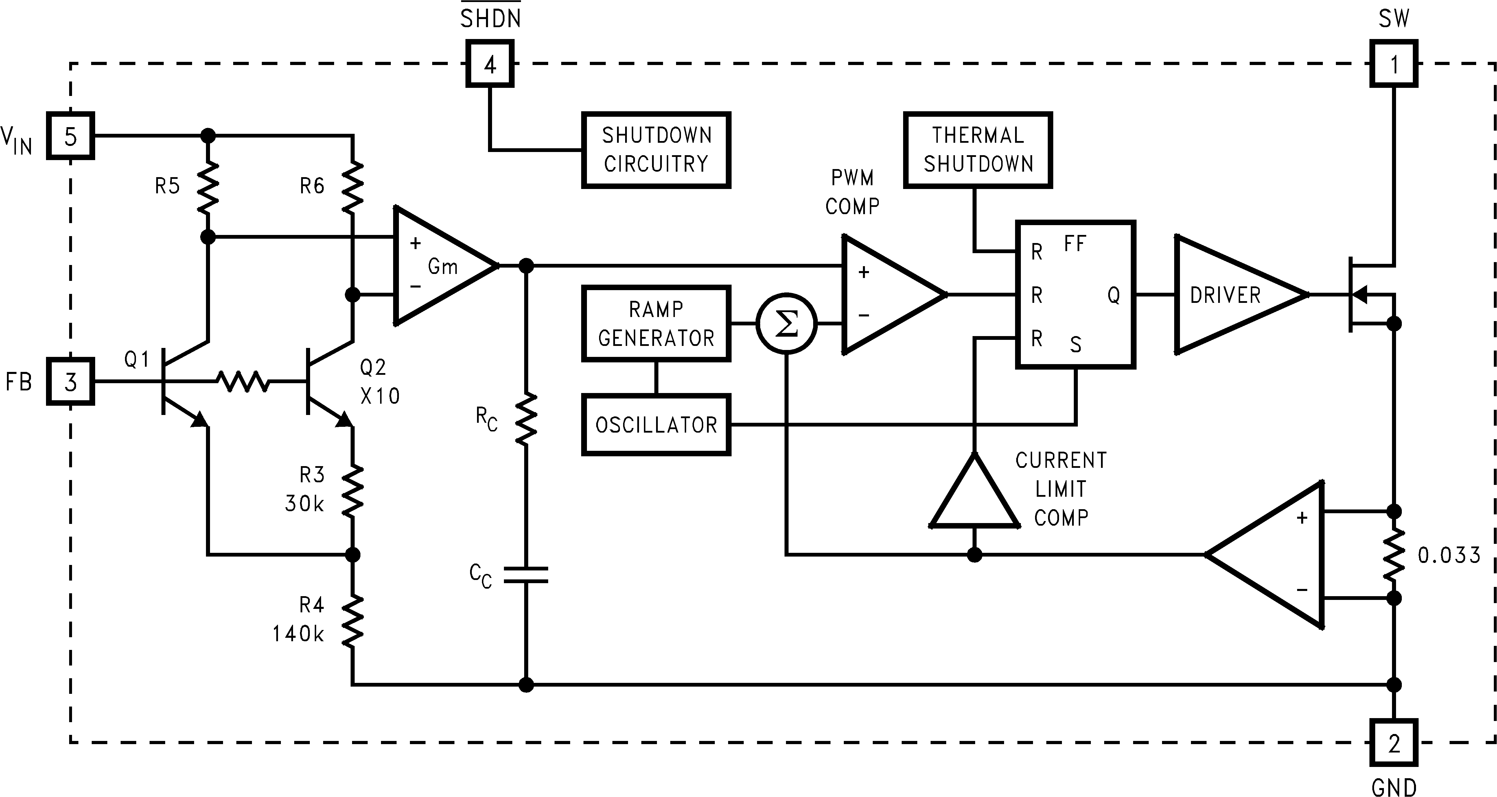
The LM2731 device is a switching converter IC that operates at a fixed frequency (0.6 or 1.6 MHz) for fast transient response over a wide input voltage range and incorporates pulse-by-pulse current limiting protection. Because this is current mode control, a 33-mΩ sense resistor in series with the switch FET is used to provide a voltage (which is proportional to the FET current) to both the input of the pulse width modulation (PWM) comparator and the current limit amplifier.
7.1.1 Theory of Operation
At the beginning of each cycle, the S-R latch turns on the FET. As the current through the FET increases, a voltage (proportional to this current) is summed with the ramp coming from the ramp generator and then fed into the input of the PWM comparator. When this voltage exceeds the voltage on the other input (coming from the Gm amplifier), the latch resets and turns the FET off. Because the signal coming from the Gm amplifier is derived from the feedback (which samples the voltage at the output), the action of the PWM comparator constantly sets the correct peak current through the FET to keep the output voltage in regulation.
Q1 and Q2 along with R3 - R6 form a bandgap voltage reference used by the IC to hold the output in regulation. The currents flowing through Q1 and Q2 will be equal, and the feedback loop will adjust the regulated output to maintain this. Because of this, the regulated output is always maintained at a voltage level equal to the voltage at the FB node "multiplied up" by the ratio of the output resistive-divider.
The current limit comparator feeds directly into the flip-flop that drives the switch FET. If the FET current reaches the limit threshold, the FET is turned off and the cycle terminated until the next clock pulse. The current limit input terminates the pulse regardless of the status of the output of the PWM comparator.
7.2 Functional Block Diagram

7.3 Feature Description
The LM2731 is a fixed-frequency boost regulator IC that delivers a minimum 1.8-A peak switch current.
The device provides cycle-by-cycle current limit protection as well as thermal shutdown protection. The device can also be controlled through the shutdown pin.
7.4 Device Functional Modes
7.4.1 Shutdown Pin Operation
The device is turned off by pulling the shutdown pin low. If this function is not going to be used, the pin should be tied directly to VIN. If the SHDN function will be needed, a pullup resistor must be used to VIN (approximately 50 kΩ to 100 kΩ recommended). The SHDN pin must not be left unterminated.
7.4.2 Thermal Shutdown
Thermal shutdown limits total power dissipation by turning off the output switch when the IC junction temperature exceeds 160°C. After thermal shutdown occurs, the output switch doesn’t turn on until the junction temperature drops to approximately 150°C.
7.4.3 Current Limit
The LM2731 uses cycle-by-cycle current limiting to protect the internal NMOS switch. It is important to note that this current limit will not protect the output from excessive current during an output short-circuit. The input supply is connected to the output by the series connection of an inductor and a diode. If a short circuit is placed on the output, excessive current can damage both the inductor and diode.