SNVS487E December 2006 – January 2015 LM27313 , LM27313-Q1
PRODUCTION DATA.
- 1 Features
- 2 Applications
- 3 Description
- 4 Revision History
- 5 Pin Configuration and Functions
- 6 Specifications
- 7 Detailed Description
-
8 Application and Implementation
- 8.1 Application Information
- 8.2
Typical Applications
- 8.2.1
Application Circuit VIN=5.0 V, VOUT=12.0 V, Iload=250 mA
- 8.2.1.1 Design Requirements
- 8.2.1.2
Detailed Design Procedure
- 8.2.1.2.1 Selecting the External Capacitors
- 8.2.1.2.2 Selecting the Output Capacitor
- 8.2.1.2.3 Selecting the Input Capacitor
- 8.2.1.2.4 Feed-Forward Compensation
- 8.2.1.2.5 Selecting Diodes
- 8.2.1.2.6 Setting the Output Voltage
- 8.2.1.2.7 Duty Cycle
- 8.2.1.2.8 Inductance Value
- 8.2.1.2.9 Maximum Switch Current
- 8.2.1.2.10 Calculating Load Current
- 8.2.1.2.11 Design Parameters VSW and ISW
- 8.2.1.2.12 Minimum Inductance
- 8.2.1.2.13 Inductor Suppliers
- 8.2.1.2.14 Shutdown Pin Operation
- 8.2.1.3 Application Curves
- 8.2.2 Application Circuit VIN=5.0V, VOUT=20.0V, Iload=150mA
- 8.2.1
Application Circuit VIN=5.0 V, VOUT=12.0 V, Iload=250 mA
- 9 Power Supply Recommendations
- 10Layout
- 11Device and Documentation Support
- 12Mechanical, Packaging, and Orderable Information
Package Options
Mechanical Data (Package|Pins)
- DBV|5
Thermal pad, mechanical data (Package|Pins)
Orderable Information
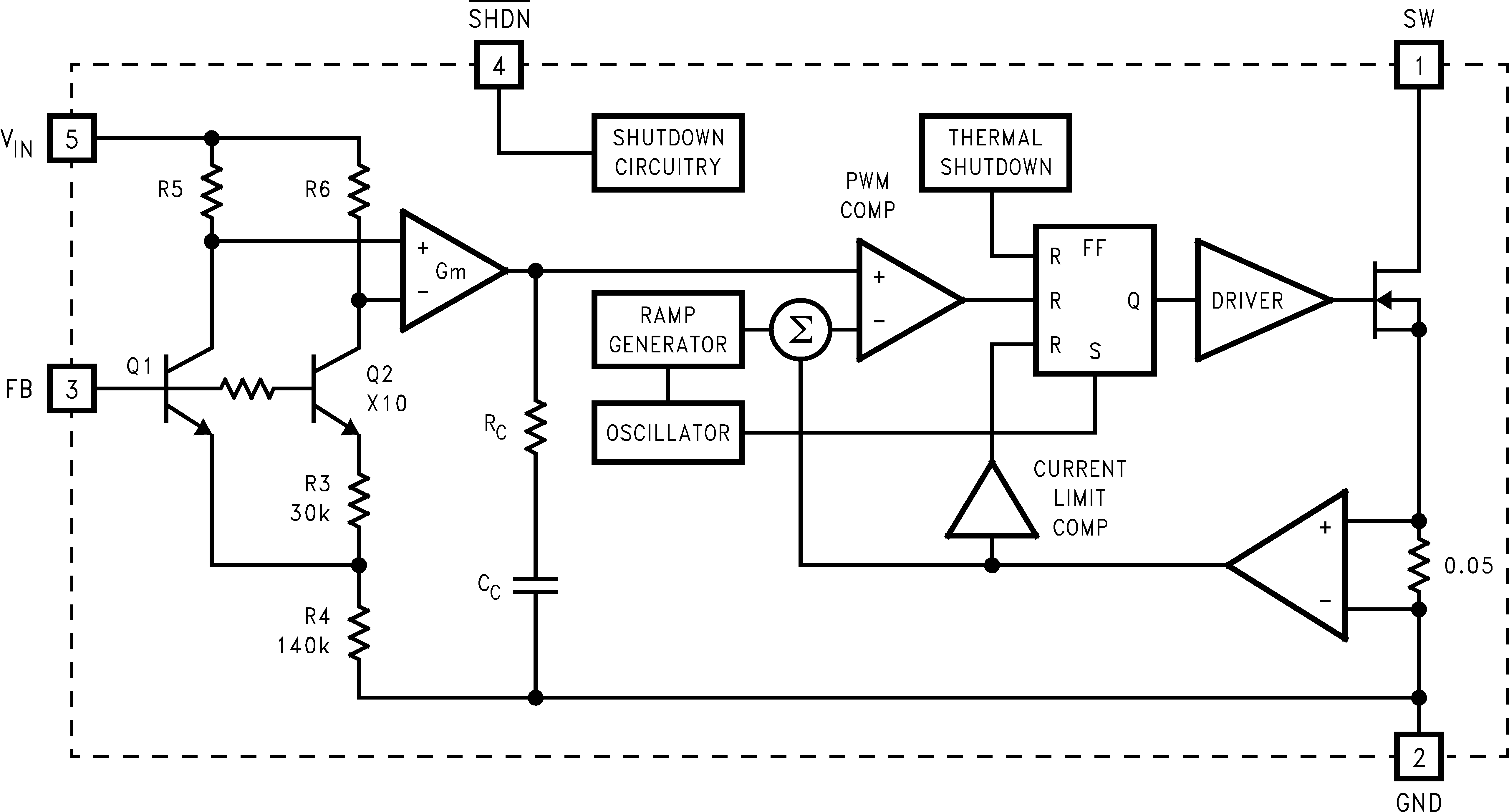
7 Detailed Description
7.1 Overview
The LM27313 is a switching converter IC that operates at a fixed frequency of 1.6 MHz using current-mode control for fast transient response over a wide input voltage range and incorporate pulse-by-pulse current limiting protection. Because this is current mode control, a 50-mΩ sense resistor in series with the switch FET is used to provide a voltage (which is proportional to the FET current) to both the input of the pulse width modulation (PWM) comparator and the current limit amplifier.
At the beginning of each cycle, the S-R latch turns on the FET. As the current through the FET increases, a voltage (proportional to this current) is summed with the ramp coming from the ramp generator and then fed into the input of the PWM comparator. When this voltage exceeds the voltage on the other input (coming from the Gm amplifier), the latch resets and turns the FET off. Because the signal coming from the Gm amplifier is derived from the feedback (which samples the voltage at the output), the action of the PWM comparator constantly sets the correct peak current through the FET to keep the output voltage in regulation.
Q1 and Q2 along with R3 - R6 form a bandgap voltage reference used by the IC to hold the output in regulation. The currents flowing through Q1 and Q2 will be equal, and the feedback loop will adjust the regulated output to maintain this. Because of this, the regulated output is always maintained at a voltage level equal to the voltage at the FB node "multiplied up" by the ratio of the output resistive divider.
The current limit comparator feeds directly into the flip-flop, that drives the switch FET. If the FET current reaches the limit threshold, the FET is turned off and the cycle terminated until the next clock pulse. The current limit input terminates the pulse regardless of the status of the output of the PWM comparator.
7.2 Functional Block Diagram
7.3 Feature Description
This device is designed as a current mode boost converter for a wide input voltage range. It features a very small package and operates at a high switching frequency. This allows for use of small passive components (inductors and capacitors), enabling small solution size. The device features also logic level shutdown, making it ideal for applications where low power consumption is desired. Control loop compensation is internal and no additional external components are required. Additional protection features are provided by deploying cycle-by-cycle current limiting and thermal shutdown.
7.4 Device Functional Modes
In normal operational mode, the device regulates output voltage to the value set with resistive divider. In addition, this device has a logic level shutdown pin (SHDN) that allows user to turn the device on/off by driving this pin high/low. Default setup is that this pin is connected to VIN through pullup resistor (typically 50 kΩ). When shutdown pin is low, the device is in shutdown mode consuming typically only 24 nA, making it ideal for applications where low power consumption is desirable.