SNVS316H September 2004 – December 2014 LM2736
PRODUCTION DATA.
- 1 Features
- 2 Applications
- 3 Description
- 4 Revision History
- 5 Pin Configuration and Functions
- 6 Specifications
- 7 Detailed Description
-
8 Application and Implementation
- 8.1 Application Information
- 8.2
Typical Applications
- 8.2.1 LM2736X (1.6 MHz) VBOOST Derived from VIN 5 V to 1.5 V / 750 mA
- 8.2.2 LM2736X (1.6 MHz) VBOOST Derived from VOUT 12 V to 3.3 V / 750 mA
- 8.2.3 LM2736X (1.6 MHz) VBOOST Derived from VSHUNT 18 V to 1.5 V / 750 mA
- 8.2.4 LM2736X (1.6 MHz) VBOOST Derived from Series Zener Diode (VIN) 15 V to 1.5 V / 750 mA
- 8.2.5 LM2736X (1.6 MHz) VBOOST Derived from Series Zener Diode (VOUT) 15 V to 9 V / 750 mA
- 8.2.6 LM2736Y (550 kHz) VBOOST Derived from VIN 5 V to 1.5 V / 750 mA
- 8.2.7 LM2736Y (550 kHz) VBOOST Derived from VOUT 12 V to 3.3 V / 750 mA
- 8.2.8 LM2736Y (550 kHz) VBOOST Derived from VSHUNT 18 V to 1.5 V / 750 mA
- 8.2.9 LM2736Y (550 kHz) VBOOST Derived from Series Zener Diode (VIN) 15 V to 1.5 V / 750 mA
- 8.2.10 LM2736Y (550 kHz) VBOOST Derived from Series Zener Diode (VOUT) 15 V to 9 V / 750 mA
- 9 Power Supply Recommendations
- 10Layout
- 11Device and Documentation Support
- 12Mechanical, Packaging, and Orderable Information
Package Options
Mechanical Data (Package|Pins)
- DDC|6
Thermal pad, mechanical data (Package|Pins)
Orderable Information
8 Application and Implementation
NOTE
Information in the following applications sections is not part of the TI component specification, and TI does not warrant its accuracy or completeness. TI’s customers are responsible for determining suitability of components for their purposes. Customers should validate and test their design implementation to confirm system functionality.
8.1 Application Information
8.1.1 Boost Function
Capacitor CBOOST and diode D2 in Figure 12 are used to generate a voltage VBOOST. VBOOST - VSW is the gate drive voltage to the internal NMOS control switch. To properly drive the internal NMOS switch during its on-time, VBOOST needs to be at least 1.6 V greater than VSW. Although the LM2736 device will operate with this minimum voltage, it may not have sufficient gate drive to supply large values of output current. Therefore, it is recommended that VBOOST be greater than 2.5 V above VSW for best efficiency. VBOOST – VSW should not exceed the maximum operating limit of 5.5 V.
5.5 V > VBOOST – VSW > 2.5 V for best performance.
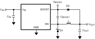 Figure 12. VOUT Charges CBOOST
When the LM2736 device starts up, internal circuitry from the BOOST pin supplies a maximum of 20 mA to CBOOST. This current charges CBOOST to a voltage sufficient to turn the switch on. The BOOST pin will continue to source current to CBOOST until the voltage at the feedback pin is greater than 1.18 V.
There are various methods to derive VBOOST:
- From the input voltage (VIN)
- From the output voltage (VOUT)
- From an external distributed voltage rail (VEXT)
- From a shunt or series zener diode
In the Functional Block Diagram, capacitor CBOOST and diode D2 supply the gate-drive current for the NMOS switch. Capacitor CBOOST is charged via diode D2 by VIN. During a normal switching cycle, when the internal NMOS control switch is off (TOFF) (refer to Figure 11), VBOOST equals VIN minus the forward voltage of D2 (VFD2), during which the current in the inductor (L) forward biases the Schottky diode D1 (VFD1). Therefore the voltage stored across CBOOST is
When the NMOS switch turns on (TON), the switch pin rises to
forcing VBOOST to rise thus reverse biasing D2. The voltage at VBOOST is then
which is approximately
for many applications. Thus the gate-drive voltage of the NMOS switch is approximately
An alternate method for charging CBOOST is to connect D2 to the output as shown in Figure 12. The output voltage should be between 2.5 V and 5.5 V, so that proper gate voltage will be applied to the internal switch. In this circuit, CBOOST provides a gate drive voltage that is slightly less than VOUT.
In applications where both VIN and VOUT are greater than 5.5 V, or less than 3 V, CBOOST cannot be charged directly from these voltages. If VIN and VOUT are greater than 5.5 V, CBOOST can be charged from VIN or VOUT minus a zener voltage by placing a zener diode D3 in series with D2, as shown in Figure 13. When using a series zener diode from the input, ensure that the regulation of the input supply doesn’t create a voltage that falls outside the recommended VBOOST voltage.
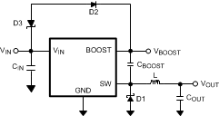 Figure 13. Zener Reduces Boost Voltage from VIN
An alternative method is to place the zener diode D3 in a shunt configuration as shown in Figure 14. A small 350 mW to 500 mW 5.1 V zener in a SOT or SOD package can be used for this purpose. A small ceramic capacitor such as a 6.3 V, 0.1 µF capacitor (C4) should be placed in parallel with the zener diode. When the internal NMOS switch turns on, a pulse of current is drawn to charge the internal NMOS gate capacitance. The 0.1 µF parallel shunt capacitor ensures that the VBOOST voltage is maintained during this time.
Resistor R3 should be chosen to provide enough RMS current to the zener diode (D3) and to the BOOST pin. A recommended choice for the zener current (IZENER) is 1 mA. The current IBOOST into the BOOST pin supplies the gate current of the NMOS control switch and varies typically according to the following formula for the X - version:
IBOOST can be calculated for the Y version using the following:
where D is the duty cycle, VZENER and VD2 are in volts, and IBOOST is in milliamps. VZENER is the voltage applied to the anode of the boost diode (D2), and VD2 is the average forward voltage across D2. Note that this formula for IBOOST gives typical current. For the worst case IBOOST, increase the current by 40%. In that case, the worst case boost current will be
R3 will then be given by
For example, using the X-version let VIN = 10 V, VZENER = 5 V, VD2 = 0.7 V, IZENER = 1 mA, and duty cycle D = 50%. Then
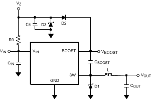 Figure 14. Boost Voltage Supplied from the Shunt Zener on VIN
8.2 Typical Applications
8.2.1 LM2736X (1.6 MHz) VBOOST Derived from VIN 5 V to 1.5 V / 750 mA
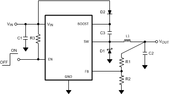 Figure 15. LM2736X (1.6 MHz) VBOOST Derived from VIN 5 V to 1.5 V / 750 mA
8.2.1.1 Design Requirements
Derive charge for VBOOST from the input supply (VIN). VBOOST – VSW should not exceed the maximum operating limit of 5.5 V.
8.2.1.2 Detailed Design Procedures
Table 1. Bill of Materials for Figure 15
| PART ID | PART VALUE | PART NUMBER | MANUFACTURER |
|---|---|---|---|
| U1 | 750 mA Buck Regulator | LM2736X | TI |
| C1, Input Cap | 10-µF, 6.3V, X5R | C3216X5ROJ106M | TDK |
| C2, Output Cap | 10-µF, 6.3V, X5R | C3216X5ROJ106M | TDK |
| C3, Boost Cap | 0.01-uF, 16V, X7R | C1005X7R1C103K | TDK |
| D1, Catch Diode | 0.3 VF Schottky 1 A, 10 VR | MBRM110L | ON Semi |
| D2, Boost Diode | 1 VF @ 50 mA Diode | 1N4148W | Diodes, Inc. |
| L1 | 4.7-µH, 1.7 A, | VLCF4020T- 4R7N1R2 | TDK |
| R1 | 2 kΩ, 1% | CRCW06032001F | Vishay |
| R2 | 10 kΩ, 1% | CRCW06031002F | Vishay |
| R3 | 100 kΩ, 1% | CRCW06031003F | Vishay |
8.2.1.2.1 Inductor Selection
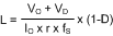
The Duty Cycle (D) can be approximated quickly using the ratio of output voltage (VO) to input voltage (VIN) as shown in Equation 14:

The catch diode (D1) forward voltage drop and the voltage drop across the internal NMOS must be included to calculate a more accurate duty cycle. Use Equation 15 to Calculate D.

VSW can be approximated by:
The diode forward drop (VD) can range from 0.3 V to 0.7 V depending on the quality of the diode. The lower VD is, the higher the operating efficiency of the converter.
The inductor value determines the output ripple current. Lower inductor values decrease the size of the inductor, but increase the output ripple current. An increase in the inductor value will decrease the output ripple current. The ratio of ripple current (ΔiL) to output current (IO) is optimized when it is set between 0.3 and 0.4 at 750 mA. The ratio r is defined in .

One must also ensure that the minimum current limit (1.0 A) is not exceeded, so the peak current in the inductor must be calculated. Use Equation 18 to calculate the peak current (ILPK) in the inductor.
If r = 0.7 at an output of 750 mA, the peak current in the inductor will be 1.0125 A. The minimum ensured current limit over all operating conditions is 1.0 A. One can either reduce r to 0.6 resulting in a 975 mA peak current, or make the engineering judgement that 12.5 mA over will be safe enough with a 1.5 A typical current limit and 6 sigma limits. When the designed maximum output current is reduced, the ratio r can be increased. At a current of 0.1 A, r can be made as high as 0.9. The ripple ratio can be increased at lighter loads because the net ripple is actually quite low, and if r remains constant the inductor value can be made quite large. Equation 19 is empirically developed for the maximum ripple ratio at any current below 2 A.
Note that this is just a guideline.
The LM2736 device operates at frequencies allowing the use of ceramic output capacitors without compromising transient response. Ceramic capacitors allow higher inductor ripple without significantly increasing output ripple. See the Output Capacitor section for more details on calculating output voltage ripple.
Now that the ripple current or ripple ratio is determined, the inductance is calculated using Equation 20
where fs is the switching frequency and IO is the output current. When selecting an inductor, make sure that it is capable of supporting the peak output current without saturating. Inductor saturation will result in a sudden reduction in inductance and prevent the regulator from operating correctly. Because of the speed of the internal current limit, the peak current of the inductor need only be specified for the required maximum output current. For example, if the designed maximum output current is 0.5 A and the peak current is 0.7 A, then the inductor should be specified with a saturation current limit of >0.7 A. There is no need to specify the saturation or peak current of the inductor at the 1.5 A typical switch current limit. The difference in inductor size is a factor of 5. Because of the operating frequency of the LM2736, ferrite based inductors are preferred to minimize core losses. This presents little restriction since the variety of ferrite based inductors is huge. Lastly, inductors with lower series resistance (DCR) will provide better operating efficiency. For recommended inductors see Example Circuits.
8.2.1.2.2 Input Capacitor
An input capacitor is necessary to ensure that VIN does not drop excessively during switching transients. The primary specifications of the input capacitor are capacitance, voltage, RMS current rating, and ESL (Equivalent Series Inductance). The recommended input capacitance is 10-µF, although 4.7-µF works well for input voltages below 6 V. The input voltage rating is specifically stated by the capacitor manufacturer. Make sure to check any recommended deratings and also verify if there is any significant change in capacitance at the operating input voltage and the operating temperature. The input capacitor maximum RMS input current rating (IRMS-IN) must be greater than:
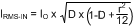
It can be shown from the above equation that maximum RMS capacitor current occurs when D = 0.5. Always calculate the RMS at the point where the duty cycle, D, is closest to 0.5. The ESL of an input capacitor is usually determined by the effective cross sectional area of the current path. A large leaded capacitor will have high ESL and a 0805 ceramic chip capacitor will have very low ESL. At the operating frequencies of the LM2736, certain capacitors may have an ESL so large that the resulting impedance (2πfL) will be higher than that required to provide stable operation. As a result, surface mount capacitors are strongly recommended. Sanyo POSCAP, Tantalum or Niobium, Panasonic SP or Cornell Dubilier ESR, and multilayer ceramic capacitors (MLCC) are all good choices for both input and output capacitors and have very low ESL. For MLCCs it is recommended to use X7R or X5R dielectrics. Consult capacitor manufacturer datasheet to see how rated capacitance varies over operating conditions.
8.2.1.2.3 Output Capacitor
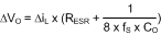
The output capacitor is selected based upon the desired output ripple and transient response. The initial current of a load transient is provided mainly by the output capacitor. The output ripple of the converter is:
When using MLCCs, the ESR is typically so low that the capacitive ripple may dominate. When this occurs, the output ripple will be approximately sinusoidal and 90° phase shifted from the switching action. Given the availability and quality of MLCCs and the expected output voltage of designs using the LM2736, there is really no need to review any other capacitor technologies. Another benefit of ceramic capacitors is their ability to bypass high frequency noise. A certain amount of switching edge noise will couple through parasitic capacitances in the inductor to the output. A ceramic capacitor will bypass this noise while a tantalum will not. Since the output capacitor is one of the two external components that control the stability of the regulator control loop, most applications will require a minimum at 10-µF of output capacitance. Capacitance can be increased significantly with little detriment to the regulator stability. Like the input capacitor, recommended multilayer ceramic capacitors are X7R or X5R. Again, verify actual capacitance at the desired operating voltage and temperature.
Check the RMS current rating of the capacitor. The RMS current rating of the capacitor chosen must also meet the following condition:

8.2.1.2.4 Catch Diode
The catch diode (D1) conducts during the switch off-time. A Schottky diode is recommended for its fast switching times and low forward voltage drop. The catch diode should be chosen so that its current rating is greater than:
The reverse breakdown rating of the diode must be at least the maximum input voltage plus appropriate margin. To improve efficiency choose a Schottky diode with a low forward voltage drop.
8.2.1.2.5 Boost Diode
A standard diode such as the 1N4148 type is recommended. For VBOOST circuits derived from voltages less than 3.3 V, a small-signal Schottky diode is recommended for greater efficiency. A good choice is the BAT54 small signal diode.
8.2.1.2.6 Boost Capacitor
A ceramic 0.01-µF capacitor with a voltage rating of at least 16 V is sufficient. The X7R and X5R MLCCs provide the best performance.
8.2.1.2.7 Output Voltage
The output voltage is set using the following equation where R2 is connected between the FB pin and GND, and R1 is connected between VO and the FB pin. A good value for R2 is 10 kΩ.

8.2.1.3 Application Curves
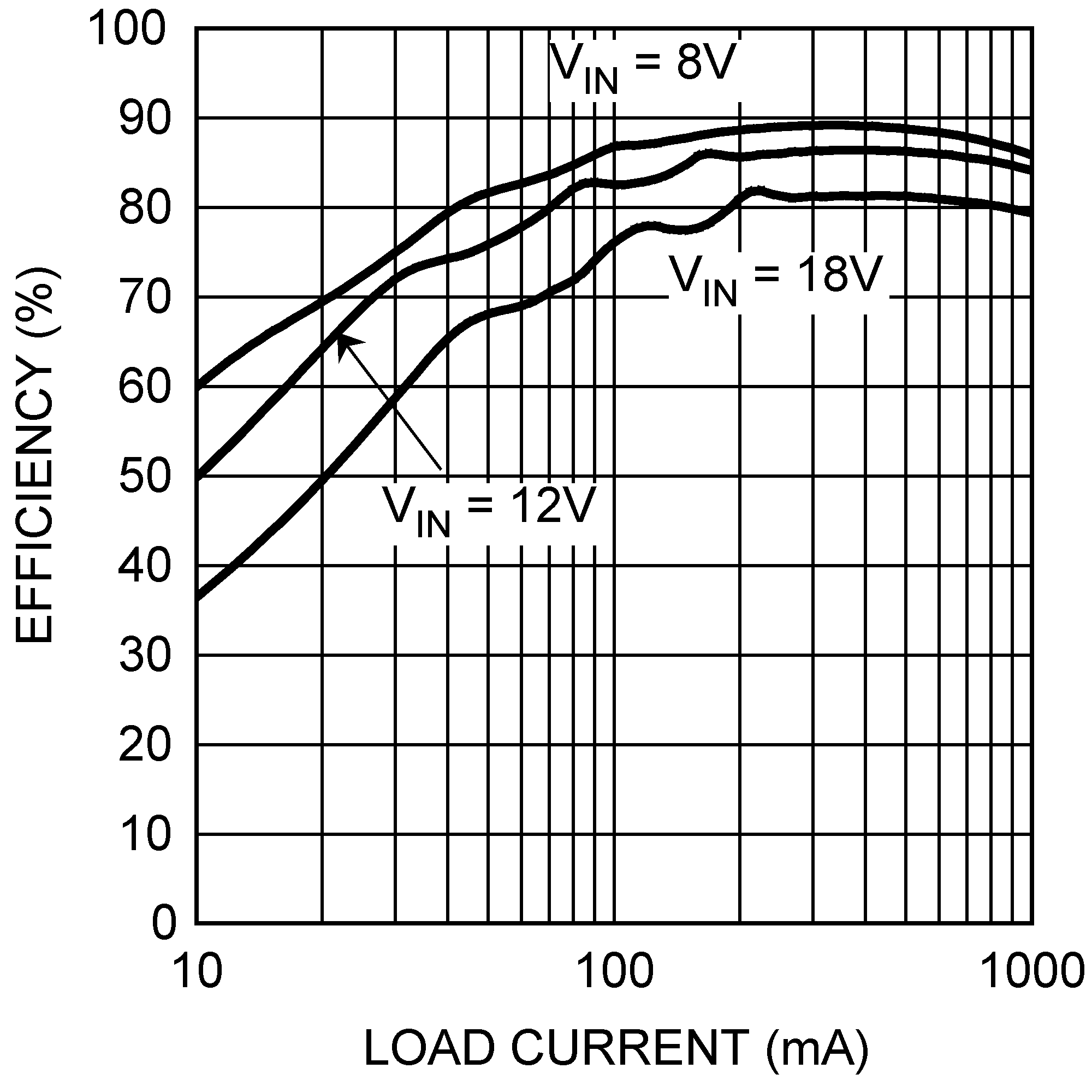
| VOUT = 5 V |
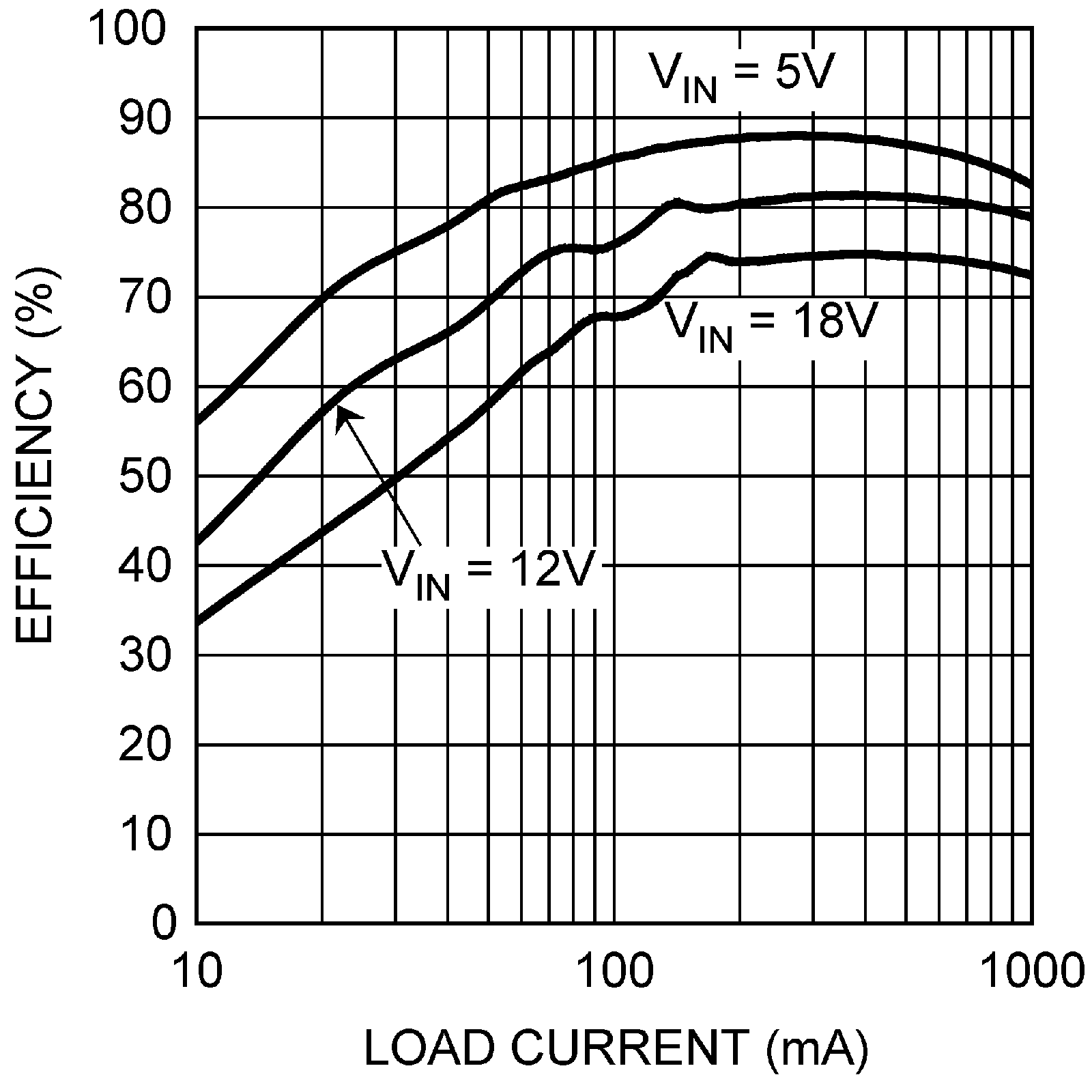
| VOUT = 3.3 V |
| VOUT = 1.5 V |
| VOUT = 5 V |
| VOUT = 3.3 V |
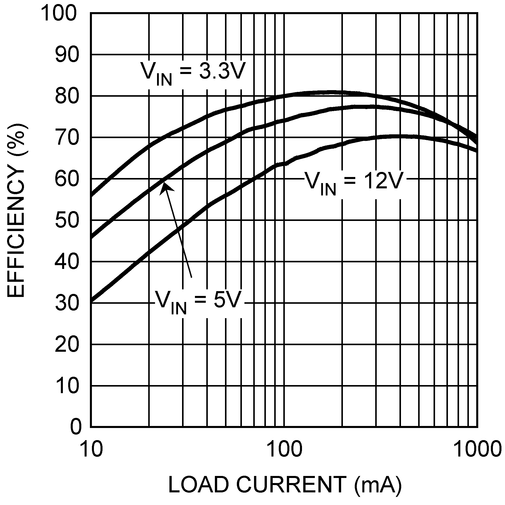
| VOUT = 1.5 V |
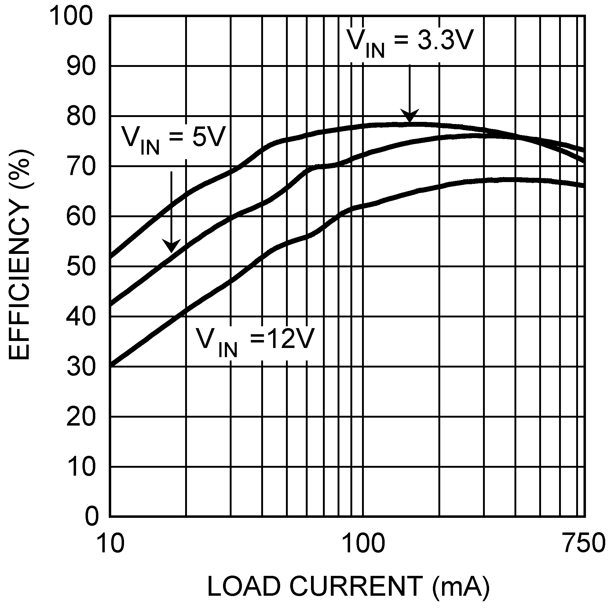
8.2.2 LM2736X (1.6 MHz) VBOOST Derived from VOUT 12 V to 3.3 V / 750 mA
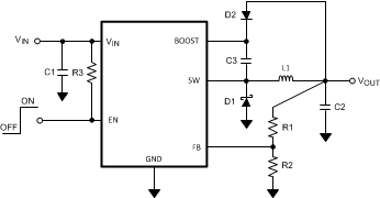 Figure 22. LM2736X (1.6 MHz) VBOOST Derived from VOUT 12 V to 3.3 V / 750 mA
8.2.2.1 Design Requirements
Derive charge for VBOOST from the output voltage, (VOUT). The output voltage should be between 2.5V and 5.5V.
8.2.2.2 Detailed Design Procedures
Table 2. Bill of Materials for Figure 22
| PART ID | PART VALUE | PART NUMBER | MANUFACTURER |
|---|---|---|---|
| U1 | 750mA Buck Regulator | LM2736X | TI |
| C1, Input Cap | 10µF, 25V, X7R | C3225X7R1E106M | TDK |
| C2, Output Cap | 22µF, 6.3V, X5R | C3216X5ROJ226M | TDK |
| C3, Boost Cap | 0.01µF, 16V, X7R | C1005X7R1C103K | TDK |
| D1, Catch Diode | 0.34VF Schottky 1A, 30VR | SS1P3L | Vishay |
| D2, Boost Diode | 30V, 200 mA Schottky | BAT54 | Diodes Inc. |
| L1 | 4.7µH, 1.7A, | VLCF4020T- 4R7N1R2 | TDK |
| R1 | 16.5kΩ, 1% | CRCW06031652F | Vishay |
| R2 | 10.0 kΩ, 1% | CRCW06031002F | Vishay |
| R3 | 100kΩ, 1% | CRCW06031003F | Vishay |
Please refer to Detailed Design Procedures.
8.2.2.3 Application Curves
Please refer to Application Curves
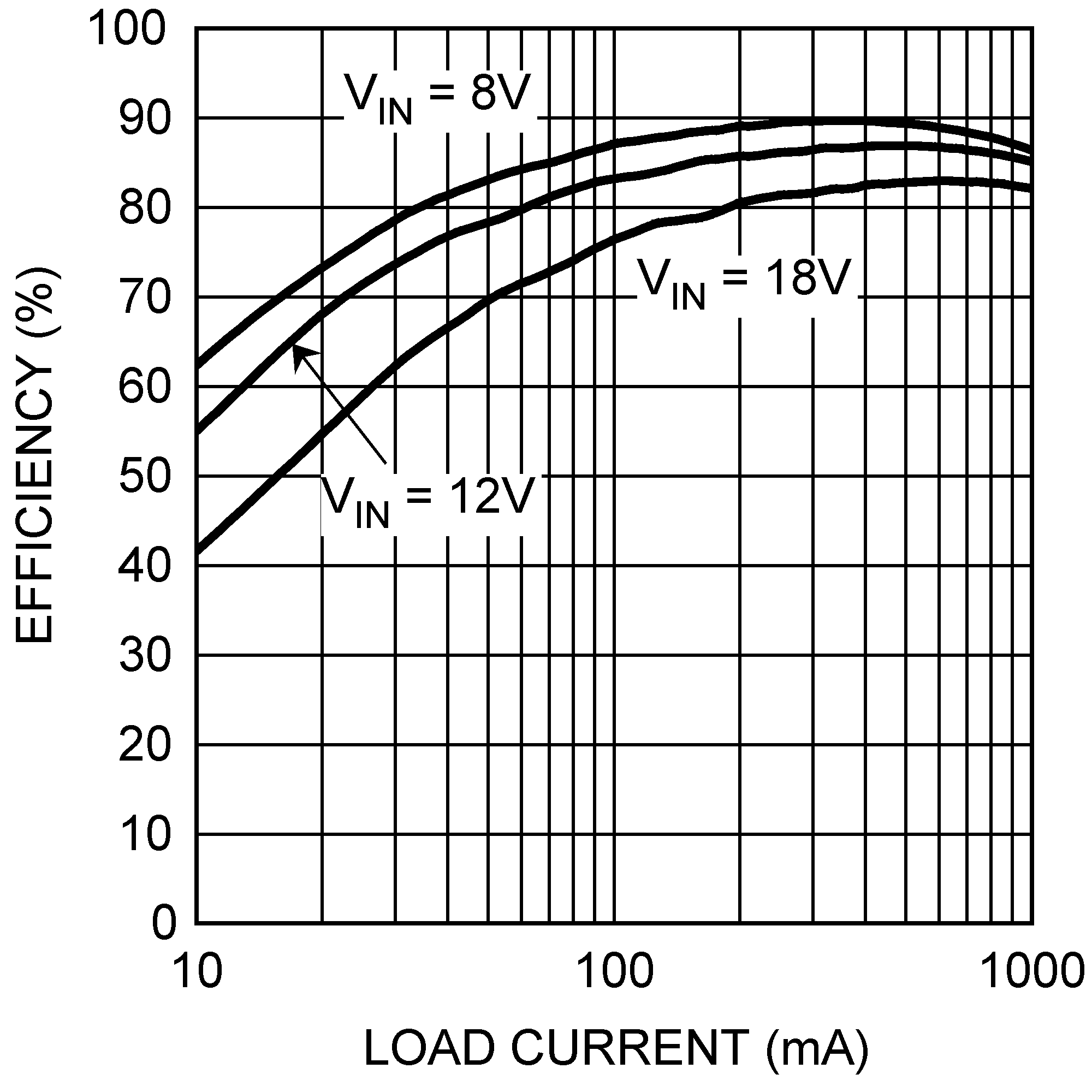
8.2.3 LM2736X (1.6 MHz) VBOOST Derived from VSHUNT 18 V to 1.5 V / 750 mA
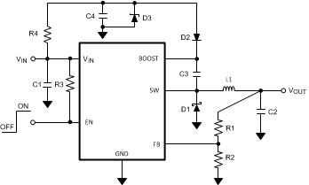 Figure 23. LM2736X (1.6 MHz) VBOOST Derived from VSHUNT 18 V to 1.5 V / 750 mA
8.2.3.1 Design Requirements
An alternative method when VIN is greater than 5.5V is to place the zener diode D3 in a shunt configuration. A small 350 mW to 500 mW 5.1 V zener in a SOT or SOD package can be used for this purpose. A small ceramic capacitor such as a 6.3 V, 0.1 µF capacitor (C4) should be placed in parallel with the zener diode. When the internal NMOS switch turns on, a pulse of current is drawn to charge the internal NMOS gate capacitance. The 0.1 µF parallel shunt capacitor ensures that the VBOOST voltage is maintained during this time
8.2.3.2 Detailed Design Procedure
Table 3. Bill of Materials for Figure 23
| PART ID | PART VALUE | PART NUMBER | MANUFACTURER |
|---|---|---|---|
| U1 | 750mA Buck Regulator | LM2736X | TI |
| C1, Input Cap | 10µF, 25V, X7R | C3225X7R1E106M | TDK |
| C2, Output Cap | 22µF, 6.3V, X5R | C3216X5ROJ226M | TDK |
| C3, Boost Cap | 0.01µF, 16V, X7R | C1005X7R1C103K | TDK |
| C4, Shunt Cap | 0.1µF, 6.3V, X5R | C1005X5R0J104K | TDK |
| D1, Catch Diode | 0.4VF Schottky 1A, 30VR | SS1P3L | Vishay |
| D2, Boost Diode | 1VF @ 50mA Diode | 1N4148W | Diodes, Inc. |
| D3, Zener Diode | 5.1V 250Mw SOT | BZX84C5V1 | Vishay |
| L1 | 6.8µH, 1.6A, | SLF7032T-6R8M1R6 | TDK |
| R1 | 2kΩ, 1% | CRCW06032001F | Vishay |
| R2 | 10kΩ, 1% | CRCW06031002F | Vishay |
| R3 | 100kΩ, 1% | CRCW06031003F | Vishay |
| R4 | 4.12kΩ, 1% | CRCW06034121F | Vishay |
Please refer to Detailed Design Procedures.
8.2.3.3 Application Curves
Please refer to Application Curves.
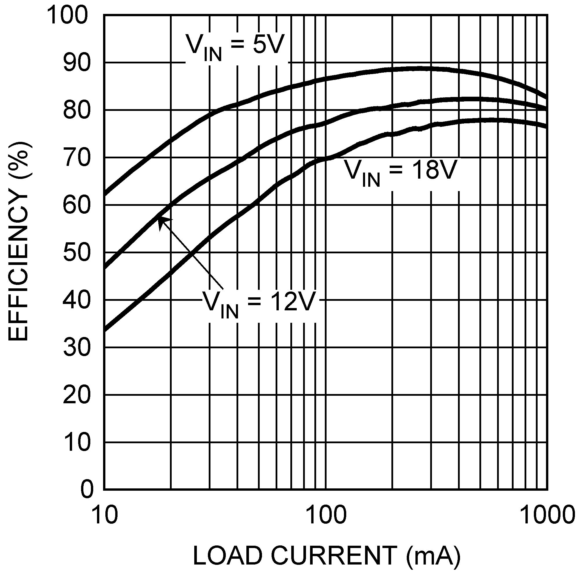
8.2.4 LM2736X (1.6 MHz) VBOOST Derived from Series Zener Diode (VIN) 15 V to 1.5 V / 750 mA
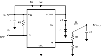 Figure 24. LM2736X (1.6 MHz) VBOOST Derived from Series Zener Diode (VIN) 15 V to 1.5 V / 750 mA
8.2.4.1 Design Requirements
In applications where both VIN and VOUT are greater than 5.5 V, or less than 3 V, CBOOST cannot be charged directly from these voltages. If VIN is greater than 5.5 V, CBOOST can be charged from VIN minus a zener voltage by placing a zener diode D3 in series with D2. When using a series zener diode from the input, ensure that the regulation of the input supply doesn’t create a voltage that falls outside the recommended VBOOST voltage.
8.2.4.2 Detailed Design Procedure
Table 4. Bill of Materials for Figure 24
| PART ID | PART VALUE | PART NUMBER | MANUFACTURER |
|---|---|---|---|
| U1 | 750 mA Buck Regulator | LM2736X | TI |
| C1, Input Cap | 10-µF, 25 V, X7R | C3225X7R1E106M | TDK |
| C2, Output Cap | 22-µF, 6.3 V, X5R | C3216X5ROJ226M | TDK |
| C3, Boost Cap | 0.01-µF, 16 V, X7R | C1005X7R1C103K | TDK |
| D1, Catch Diode | 0.4 VF Schottky 1 A, 30VR | SS1P3L | Vishay |
| D2, Boost Diode | 1VF @ 50 mA Diode | 1N4148W | Diodes, Inc. |
| D3, Zener Diode | 11 V 350 Mw SOT | BZX84C11T | Diodes, Inc. |
| L1 | 6.8µH, 1.6 A, | SLF7032T-6R8M1R6 | TDK |
| R1 | 2 kΩ, 1% | CRCW06032001F | Vishay |
| R2 | 10 kΩ, 1% | CRCW06031002F | Vishay |
| R3 | 100 kΩ, 1% | CRCW06031003F | Vishay |
Please refer to Detailed Design Procedures.
8.2.4.3 Application Curves
Please refer to Application Curves
8.2.5 LM2736X (1.6 MHz) VBOOST Derived from Series Zener Diode (VOUT) 15 V to 9 V / 750 mA
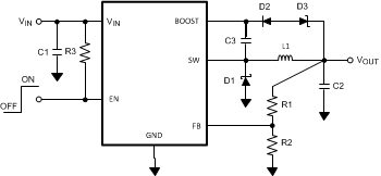 Figure 25.
8.2.5.1 Design Requirements
In applications where both VIN and VOUT are greater than 5.5 V, or less than 3 V, CBOOST cannot be charged directly from these voltages. If VIN and VOUT are greater than 5.5 V, CBOOST can be charged from VOUT minus a zener voltage by placing a zener diode D3 in series with D2.
8.2.5.2 Detailed Design Procedure
Table 5. Bill of Materials for Figure 25
| PART ID | PART VALUE | PART NUMBER | MANUFACTURER |
|---|---|---|---|
| U1 | 750mA Buck Regulator | LM2736X | TI |
| C1, Input Cap | 10µF, 25V, X7R | C3225X7R1E106M | TDK |
| C2, Output Cap | 22µF, 16V, X5R | C3216X5R1C226M | TDK |
| C3, Boost Cap | 0.01µF, 16V, X7R | C1005X7R1C103K | TDK |
| D1, Catch Diode | 0.4VF Schottky 1A, 30VR | SS1P3L | Vishay |
| D2, Boost Diode | 1VF @ 50mA Diode | 1N4148W | Diodes, Inc. |
| D3, Zener Diode | 4.3V 350mw SOT | BZX84C4V3 | Diodes, Inc. |
| L1 | 6.8µH, 1.6A, | SLF7032T-6R8M1R6 | TDK |
| R1 | 61.9kΩ, 1% | CRCW06036192F | Vishay |
| R2 | 10kΩ, 1% | CRCW06031002F | Vishay |
| R3 | 100kΩ, 1% | CRCW06031003F | Vishay |
Please refer to Detailed Design Procedures.
8.2.5.3 Application Curves
Please refer to Application Curves
8.2.6 LM2736Y (550 kHz) VBOOST Derived from VIN 5 V to 1.5 V / 750 mA
Figure 26. LM2736Y (550 kHz) VBOOST Derived from VIN 5 V to 1.5 V / 750 mA
8.2.6.1 Design Requirements
Derive charge for VBOOST from the input voltage, (VIN). VBOOST should be greater than 2.5 V above VSW for best efficiency. VBOOST – VSW should not exceed the maximum operating limit of 5.5 V.
8.2.6.2 Detailed Design Procedure
Table 6. Bill of Materials for Figure 26
| PART ID | PART VALUE | PART NUMBER | MANUFACTURER |
|---|---|---|---|
| U1 | 750mA Buck Regulator | LM2736Y | TI |
| C1, Input Cap | 10µF, 6.3V, X5R | C3216X5ROJ106M | TDK |
| C2, Output Cap | 22µF, 6.3V, X5R | C3216X5ROJ226M | TDK |
| C3, Boost Cap | 0.01µF, 16V, X7R | C1005X7R1C103K | TDK |
| D1, Catch Diode | 0.3VF Schottky 1A, 10VR | MBRM110L | ON Semi |
| D2, Boost Diode | 1VF @ 50mA Diode | 1N4148W | Diodes, Inc. |
| L1 | 10µH, 1.6A, | SLF7032T-100M1R4 | TDK |
| R1 | 2kΩ, 1% | CRCW06032001F | Vishay |
| R2 | 10kΩ, 1% | CRCW06031002F | Vishay |
| R3 | 100kΩ, 1% | CRCW06031003F | Vishay |
Please refer toDetailed Design Procedures.
8.2.6.3 Application Curves
Please refer to Application Curves.
8.2.7 LM2736Y (550 kHz) VBOOST Derived from VOUT 12 V to 3.3 V / 750 mA
Figure 27. LM2736Y (550 kHz) VBOOST Derived from VOUT 12 V to 3.3 V / 750 mA
8.2.7.1 Design Requirements
Derive charge for VBOOST from the output voltage, (VOUT). The output voltage should be between 2.5V and 5.5V.
8.2.7.2 Detailed Design Procedure
Table 7. Bill of Materials for Figure 27
| PART ID | PART VALUE | PART NUMBER | MANUFACTURER |
|---|---|---|---|
| U1 | 750mA Buck Regulator | LM2736Y | TI |
| C1, Input Cap | 10µF, 25V, X7R | C3225X7R1E106M | TDK |
| C2, Output Cap | 22µF, 6.3V, X5R | C3216X5ROJ226M | TDK |
| C3, Boost Cap | 0.01µF, 16V, X7R | C1005X7R1C103K | TDK |
| D1, Catch Diode | 0.34VF Schottky 1A, 30VR | SS1P3L | Vishay |
| D2, Boost Diode | 30V, 200 mA Schottky | BAT54 | Diodes Inc. |
| L1 | 10µH, 1.6A, | SLF7032T-100M1R4 | TDK |
| R1 | 16.5kΩ, 1% | CRCW06031652F | Vishay |
| R2 | 10.0 kΩ, 1% | CRCW06031002F | Vishay |
| R3 | 100kΩ, 1% | CRCW06031003F | Vishay |
Please refer to Detailed Design Procedures.
8.2.7.3 Application Curves
Please refer to Application Curves.
8.2.8 LM2736Y (550 kHz) VBOOST Derived from VSHUNT 18 V to 1.5 V / 750 mA
Figure 28. LM2736Y (550 kHz) VBOOST Derived from VSHUNT 18 V to 1.5 V / 750 mA
8.2.8.1 Design Requirements
An alternative method when VIN is greater than 5.5V is to place the zener diode D3 in a shunt configuration. A small 350 mW to 500 mW 5.1 V zener in a SOT or SOD package can be used for this purpose. A small ceramic capacitor such as a 6.3 V, 0.1 µF capacitor (C4) should be placed in parallel with the zener diode. When the internal NMOS switch turns on, a pulse of current is drawn to charge the internal NMOS gate capacitance. The 0.1 µF parallel shunt capacitor ensures that the VBOOST voltage is maintained during this time.
8.2.8.2 Detailed Design Procedure
Table 8. Bill of Materials for Figure 28
| PART ID | PART VALUE | PART NUMBER | MANUFACTURER |
|---|---|---|---|
| U1 | 750mA Buck Regulator | LM2736Y | TI |
| C1, Input Cap | 10µF, 25V, X7R | C3225X7R1E106M | TDK |
| C2, Output Cap | 22µF, 6.3V, X5R | C3216X5ROJ226M | TDK |
| C3, Boost Cap | 0.01µF, 16V, X7R | C1005X7R1C103K | TDK |
| C4, Shunt Cap | 0.1µF, 6.3V, X5R | C1005X5R0J104K | TDK |
| D1, Catch Diode | 0.4VF Schottky 1A, 30VR | SS1P3L | Vishay |
| D2, Boost Diode | 1VF @ 50mA Diode | 1N4148W | Diodes, Inc. |
| D3, Zener Diode | 5.1V 250Mw SOT | BZX84C5V1 | Vishay |
| L1 | 15µH, 1.5A | SLF7045T-150M1R5 | TDK |
| R1 | 2kΩ, 1% | CRCW06032001F | Vishay |
| R2 | 10kΩ, 1% | CRCW06031002F | Vishay |
| R3 | 100kΩ, 1% | CRCW06031003F | Vishay |
| R4 | 4.12kΩ, 1% | CRCW06034121F | Vishay |
Please refer to Detailed Design Procedures.
8.2.8.3 Application Curves
Please refer to Application Curves.
8.2.9 LM2736Y (550 kHz) VBOOST Derived from Series Zener Diode (VIN) 15 V to 1.5 V / 750 mA
Figure 29. M2736Y (550 kHz) VBOOST Derived from Series Zener Diode (VIN) 15 V to 1.5 V / 750 mA
8.2.9.1 Design Requirements
In applications where both VIN and VOUT are greater than 5.5 V, or less than 3 V, CBOOST cannot be charged directly from these voltages. If VIN is greater than 5.5 V, CBOOST can be charged from VIN minus a zener voltage by placing a zener diode D3 in series with D2. When using a series zener diode from the input, ensure that the regulation of the input supply doesn’t create a voltage that falls outside the recommended VBOOST voltage.
8.2.9.2 Detailed Design Procedure
Table 9. Bill of Materials for Figure 29
| PART ID | PART VALUE | PART NUMBER | MANUFACTURER |
|---|---|---|---|
| U1 | 750mA Buck Regulator | LM2736Y | TI |
| C1, Input Cap | 10µF, 25V, X7R | C3225X7R1E106M | TDK |
| C2, Output Cap | 22µF, 6.3V, X5R | C3216X5ROJ226M | TDK |
| C3, Boost Cap | 0.01µF, 16V, X7R | C1005X7R1C103K | TDK |
| D1, Catch Diode | 0.4VF Schottky 1A, 30VR | SS1P3L | Vishay |
| D2, Boost Diode | 1VF @ 50mA Diode | 1N4148W | Diodes, Inc. |
| D3, Zener Diode | 11V 350Mw SOT | BZX84C11T | Diodes, Inc. |
| L1 | 15µH, 1.5A, | SLF7045T-150M1R5 | TDK |
| R1 | 2kΩ, 1% | CRCW06032001F | Vishay |
| R2 | 10kΩ, 1% | CRCW06031002F | Vishay |
| R3 | 100kΩ, 1% | CRCW06031003F | Vishay |
Please refer to Detailed Design Procedures.
8.2.9.3 Application Curves
Please refer to Application Curves.
8.2.10 LM2736Y (550 kHz) VBOOST Derived from Series Zener Diode (VOUT) 15 V to 9 V / 750 mA
Figure 30. LM2736Y (550 kHz) VBOOST Derived from Series Zener Diode (VOUT) 15 V to 9 V / 750 mA
8.2.10.1 Design Requirements
In applications where both VIN and VOUT are greater than 5.5 V, or less than 3 V, CBOOST cannot be charged directly from these voltages. If VIN and VOUT are greater than 5.5 V, CBOOST can be charged from VOUT minus a zener voltage by placing a zener diode D3 in series with D2.
8.2.10.2 Detailed Design Procedure
Table 10. Bill of Materials for Figure 30
| PART ID | PART VALUE | PART NUMBER | MANUFACTURER |
|---|---|---|---|
| U1 | 750 mA Buck Regulator | LM2736Y | TI |
| C1, Input Cap | 10-µF, 25 V, X7R | C3225X7R1E106M | TDK |
| C2, Output Cap | 22-µF, 16 V, X5R | C3216X5R1C226M | TDK |
| C3, Boost Cap | 0.01-µF, 16 V, X7R | C1005X7R1C103K | TDK |
| D1, Catch Diode | 0.4 VF Schottky 1 A, 30 VR | SS1P3L | Vishay |
| D2, Boost Diode | 1 VF @ 50 mA Diode | 1N4148W | Diodes, Inc. |
| D3, Zener Diode | 4.3 V 350 mw SOT | BZX84C4V3 | Diodes, Inc. |
| L1 | 22 µH, 1.4 A, | SLF7045T-220M1R3-1PF | TDK |
| R1 | 61.9 kΩ, 1% | CRCW06036192F | Vishay |
| R2 | 10 kΩ, 1% | CRCW06031002F | Vishay |
| R3 | 100 kΩ, 1% | CRCW06031003F | Vishay |
Please refer to Detailed Design Procedures.
8.2.10.3 Application Curves
Please refer to Application Curves.