SNVS070D March 2000 – September 2016 LM2765
PRODUCTION DATA.
- 1 Features
- 2 Applications
- 3 Description
- 4 Revision History
- 5 Pin Configuration and Functions
- 6 Specifications
- 7 Parameter Measurement Information
- 8 Detailed Description
- 9 Application and Implementation
- 10Power Supply Recommendations
- 11Layout
- 12Device and Documentation Support
- 13Mechanical, Packaging, and Orderable Information
Package Options
Mechanical Data (Package|Pins)
- DBV|6
Thermal pad, mechanical data (Package|Pins)
Orderable Information
1 Features
- Doubles Input Supply Voltage
- SOT-23 6-Pin Package
- 20-Ω Typical Output Impedance
- 90% Typical Conversion Efficiency at 20 mA
- 0.1-µA Typical Shutdown Current
2 Applications
- Cellular Phones
- Pagers
- PDAs
- Operational Amplifier Power Supplies
- Interface Power Supplies
- Handheld Instruments
3 Description
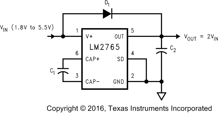
The LM2765 CMOS charge-pump voltage converter operates as a voltage doubler for an input voltage in the range of 1.8 V to 5.5 V. Two low-cost capacitors and a diode are used in this circuit to provide up to 20 mA of output current.
The LM2765 operates at 50-kHz switching frequency to reduce output resistance and voltage ripple. With an operating current of only 130 µA (operating efficiency greater than 90% with most loads) and 0.1-µA typical shutdown current, the LM2765 provides ideal performance for battery powered systems. The device is manufactured in a 6-pin SOT-23 package.
Device Information(1)
| PART NUMBER | PACKAGE | BODY SIZE (NOM) |
|---|---|---|
| LM2765 | SOT-23 (6) | 2.90 mm × 1.60 mm |
- For all available packages, see the orderable addendum at the end of the data sheet.
space
space
space
space
Voltage Doubler
