SNVS070D March 2000 – September 2016 LM2765
PRODUCTION DATA.
- 1 Features
- 2 Applications
- 3 Description
- 4 Revision History
- 5 Pin Configuration and Functions
- 6 Specifications
- 7 Parameter Measurement Information
- 8 Detailed Description
- 9 Application and Implementation
- 10Power Supply Recommendations
- 11Layout
- 12Device and Documentation Support
- 13Mechanical, Packaging, and Orderable Information
Package Options
Mechanical Data (Package|Pins)
- DBV|6
Thermal pad, mechanical data (Package|Pins)
Orderable Information
6 Specifications
6.1 Absolute Maximum Ratings
over operating free-air temperature range (unless otherwise noted)(1)(2)| MIN | MAX | UNIT | ||
|---|---|---|---|---|
| Supply voltage (V+ to GND or V+ to OUT) | 5.8 | V | ||
| SD | (GND − 0.3 V) | (V+ + 0.3 V) | ||
| OUT continuous output current | 40 | mA | ||
| Output short-circuit duration to GND(3) | 1 | sec | ||
| Continuous power dissipation (TA = 25°C)(4)
|
600 | mW | ||
| TJ-MAX(4) | 150 | °C | ||
| Storage temperature, Tstg | −65 | 150 | °C | |
(1) Stresses beyond those listed under Absolute Maximum Ratings may cause permanent damage to the device. These are stress ratings only, which do not imply functional operation of the device at these or any other conditions beyond those indicated under Recommended Operating Conditions. Exposure to absolute-maximum-rated conditions for extended periods may affect device reliability.
(2) If Military/Aerospace specified devices are required, contact the Texas Instruments Sales Office/ Distributors for availability and specifications.
(3) OUT may be shorted to GND for one second without damage. However, shorting OUT to V+ may damage the device and must be avoided. Also, for temperatures above 85°C, OUT must not be shorted to GND or V+, or device may be damaged.
(4) The maximum allowable power dissipation is calculated by using PD-MAX = (TJ-MAX − TA)/RθJA, where TJ-MAX is the maximum junction temperature, TA is the ambient temperature, and RθJA is the junction-to-ambient thermal resistance of the specified package.
6.2 ESD Ratings
| VALUE | UNIT | |||
|---|---|---|---|---|
| V(ESD) | Electrostatic discharge | Human-body model (HBM), per ANSI/ESDA/JEDEC JS-001(1) | ±2000 | V |
| Machine model | 200 | V | ||
6.3 Recommended Operating Conditions
over operating free-air temperature range (unless otherwise noted)| MIN | NOM | MAX | UNIT | ||
|---|---|---|---|---|---|
| Ambient temperature | –40 | 85 | °C | ||
| Junction temperature | –40 | 100 | °C | ||
6.4 Thermal Information
| THERMAL METRIC(1) | LM2765 | UNIT | |
|---|---|---|---|
| DBV (SOT-23) | |||
| 6 PINS | |||
| RθJA | Junction-to-ambient thermal resistance | 185.2 | °C/W |
| RθJC(top) | Junction-to-case (top) thermal resistance | 131.5 | °C/W |
| RθJB | Junction-to-board thermal resistance | 34.8 | °C/W |
| ψJT | Junction-to-top characterization parameter | 21.6 | °C/W |
| ψJB | Junction-to-board characterization parameter | 34.1 | °C/W |
(1) For more information about traditional and new thermal metrics, see the Semiconductor and IC Package Thermal Metrics application report.
6.5 Electrical Characteristics
MIN and MAX limits apply over the full operating temperature range. Unless otherwise specified: TJ = 25°C, V+ = 5 V,C1 = C2 = 3.3 μF.(1)
| PARAMETER | TEST CONDITIONS | MIN | TYP | MAX | UNIT | |
|---|---|---|---|---|---|---|
| V+ | Supply voltage | 1.8 | 5.5 | V | ||
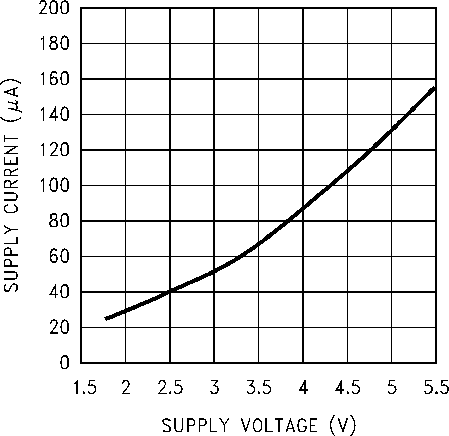
| IQ | Supply current | No load | 130 | 450 | µA | |
| ISD | Shutdown supply current | 0.1 | 0.5 | µA | ||
| TA = 85°C | 0.2 | |||||
| VSD | Shutdown pin input voltage | Shutdown mode | 2 | V | ||
| Normal operation | 0.6 | |||||
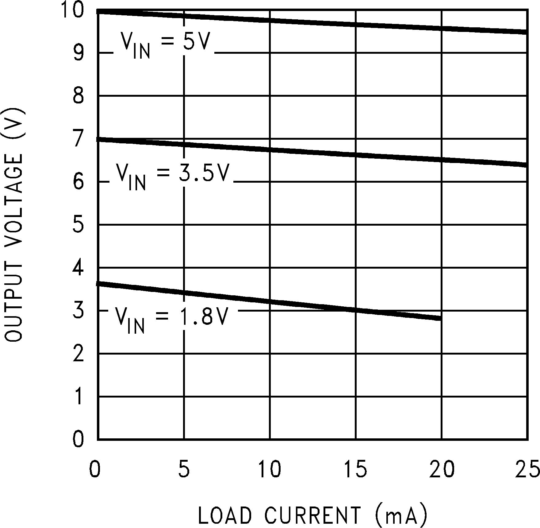
| IL | Output current | 2.5 V ≤ VIN ≤ 5.5 V | 20 | mA | ||
| 1.8 V ≤ VIN ≤ 2.5 V | 10 | |||||
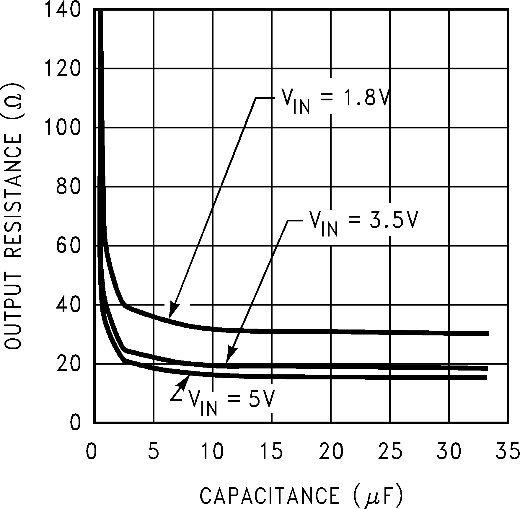
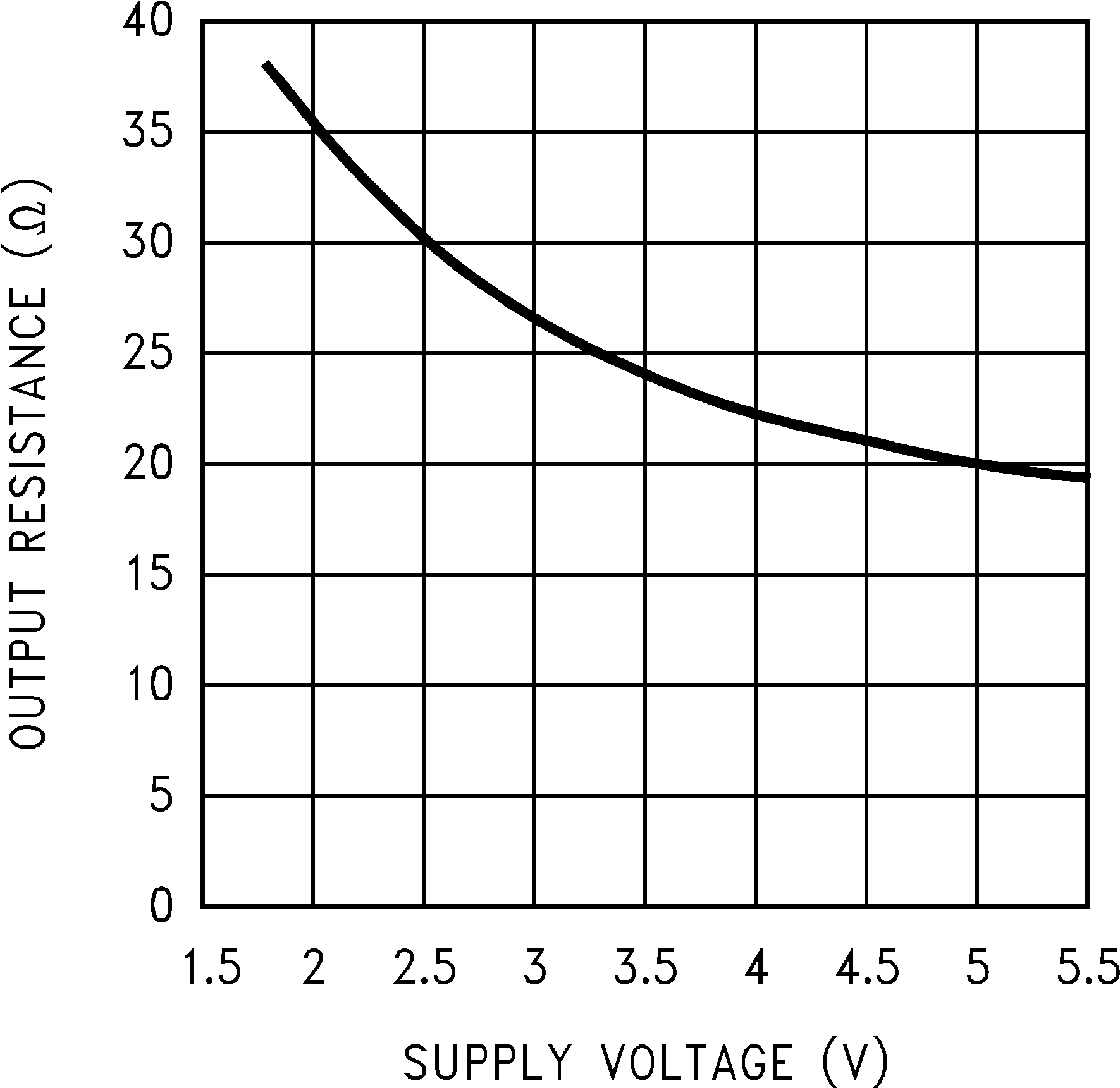
| ROUT | Output resistance(2) | IL = 20 mA | 20 | 40 | Ω | |
| ƒOSC | Oscillator frequency | See(3) | 40 | 100 | 200 | kHz |
| ƒSW | Switching frequency | See(3) | 20 | 50 | 100 | kHz |
| PEFF | Power efficiency | RL (1 kΩ) between GND and OUT | 92% | |||
| VOEFF | Voltage conversion efficiency | No load | 99.96% | |||
(1) In the test circuit, capacitors C1 and C2 are 3.3-µF, 0.3-Ω maximum ESR capacitors. Capacitors with higher ESR increase output resistance, reduce output voltage, and efficiency.
(2) Specified output resistance includes internal switch resistance and capacitor ESR. See the details in Application and Implementation for simple negative voltage converter.
(3) The output switches operate at one half of the oscillator frequency, ƒOSC = 2ƒSW.
6.6 Typical Characteristics
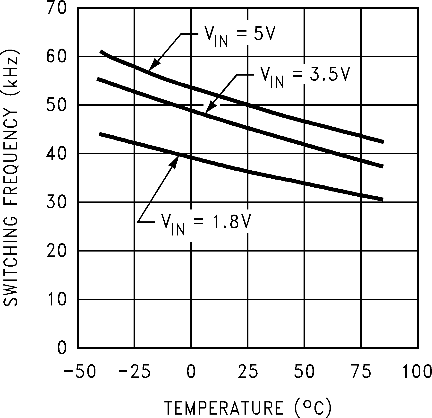
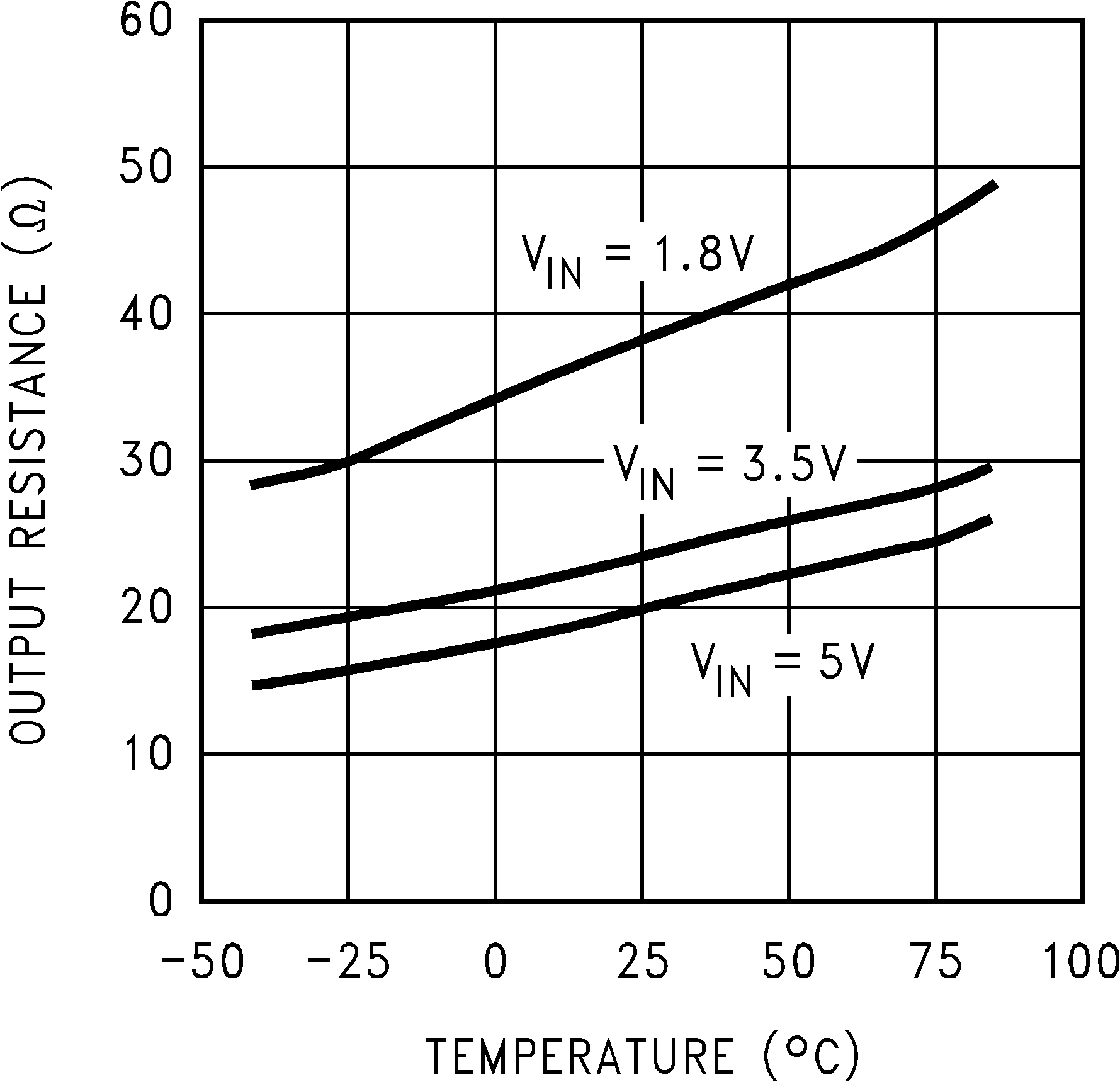
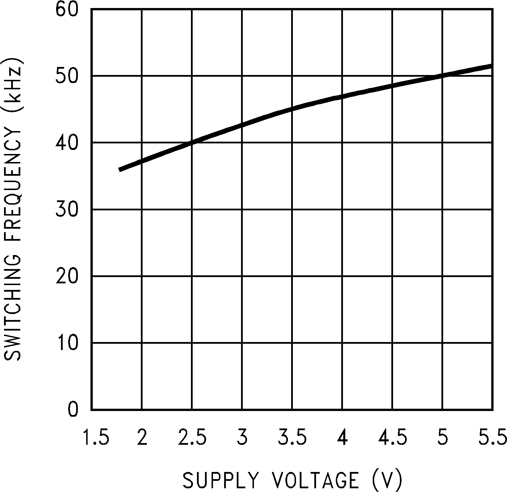
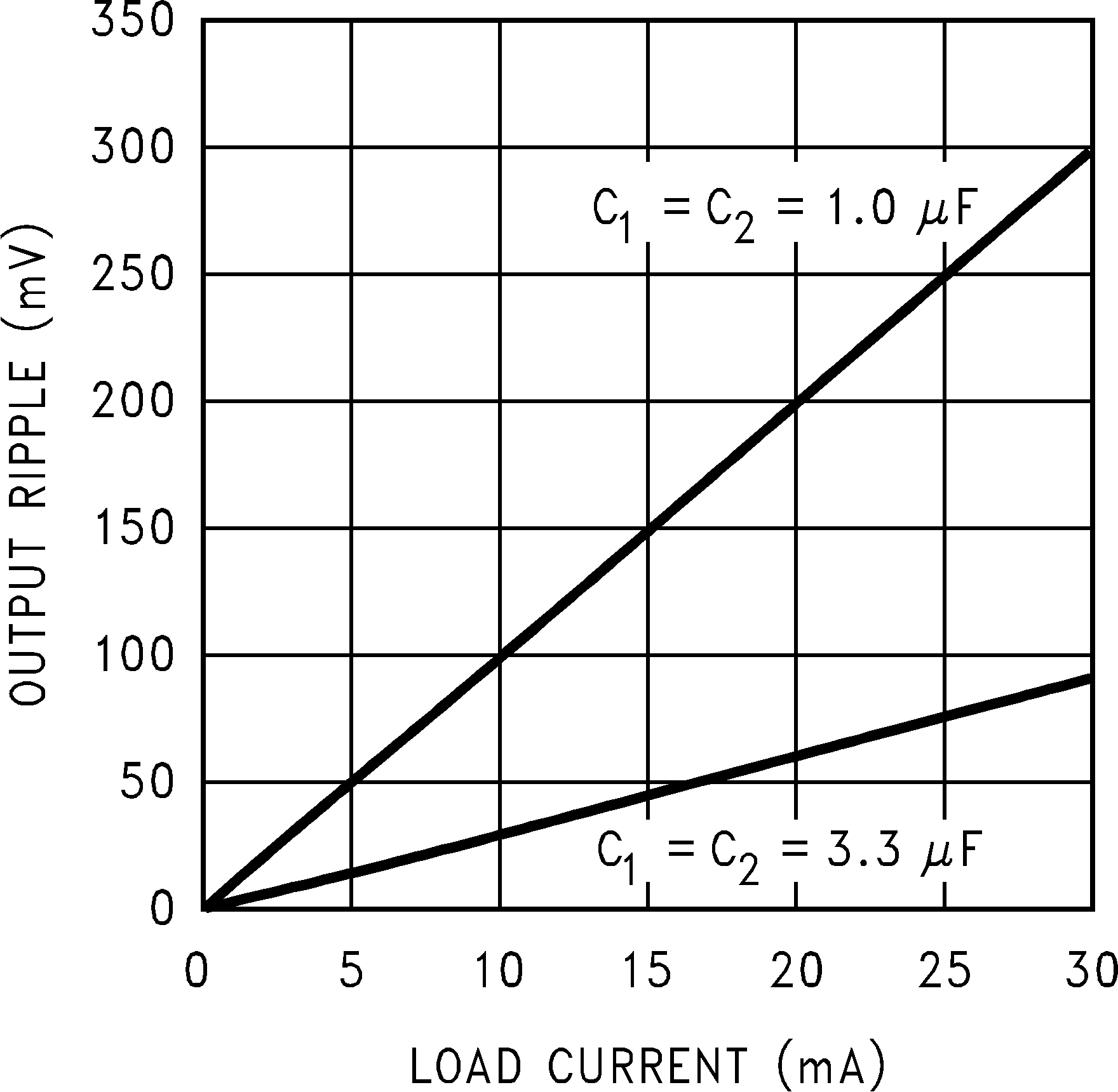
(Circuit of Test Circuit, VIN = 5V, TA = 25°C unless otherwise specified)