SNVS540K March   2009  – April 2019 LM2840 , LM2841 , LM2842

PRODUCTION DATA.  

  1. Features
  2. Applications
  3. Description
    1.     Device Images
      1.      Typical Application Circuit
  4. Revision History
  5. Pin Configuration and Functions
    1.     Pin Functions
  6. Specifications
    1. 6.1 Absolute Maximum Ratings
    2. 6.2 ESD Ratings
    3. 6.3 Recommended Operating Conditions
    4. 6.4 Thermal Information
    5. 6.5 Electrical Characteristics
    6. 6.6 Typical Characteristics
  7. Detailed Description
    1. 7.1 Overview
    2. 7.2 Functional Block Diagram
    3. 7.3 Feature Description
      1. 7.3.1 Protection
    4. 7.4 Device Functional Modes
      1. 7.4.1 Continuous Conduction Mode
  8. Application and Implementation
    1. 8.1 Application Information
    2. 8.2 Typical Applications
      1. 8.2.1 Design Requirements
      2. 8.2.2 Detailed Design Procedure
        1. 8.2.2.1 Custom Design With WEBENCH® Tools
        2. 8.2.2.2 Setting the Output Voltage
        3. 8.2.2.3 Inductor Selection
        4. 8.2.2.4 Input Capacitor
        5. 8.2.2.5 Output Capacitor
        6. 8.2.2.6 Bootstrap Capacitor
        7. 8.2.2.7 Soft-Start Components
        8. 8.2.2.8 Shutdown Operation
        9. 8.2.2.9 Schottky Diode
      3. 8.2.3 Application Curves
      4. 8.2.4 Other Application Circuits
  9. Power Supply Recommendations
  10. 10Layout
    1. 10.1 Layout Guidelines
    2. 10.2 Layout Example
  11. 11Device and Documentation Support
    1. 11.1 Device Support
      1. 11.1.1 Third-Party Products Disclaimer
      2. 11.1.2 Development Support
        1. 11.1.2.1 Custom Design With WEBENCH® Tools
    2. 11.2 Documentation Support
      1. 11.2.1 Related Documentation
    3. 11.3 Related Links
    4. 11.4 Receiving Notification of Documentation Updates
    5. 11.5 Community Resources
    6. 11.6 Trademarks
    7. 11.7 Electrostatic Discharge Caution
    8. 11.8 Glossary
  12. 12Mechanical, Packaging, and Orderable Information

Package Options

Mechanical Data (Package|Pins)
Thermal pad, mechanical data (Package|Pins)
Orderable Information

Application Curves

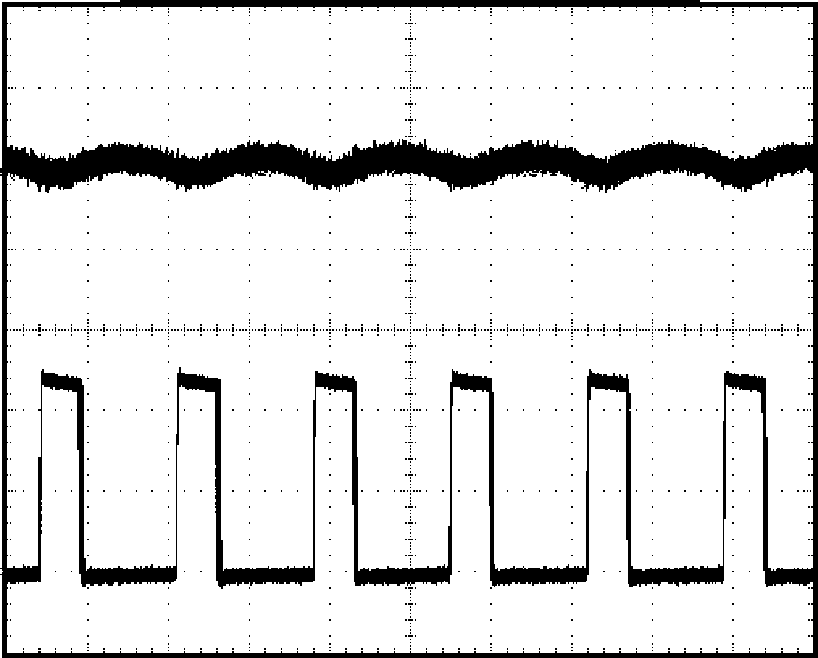
LM2840 LM2841 LM2842 30036770.png
VIN = 12 V IOUT = 200 mA
VOUT = 3.3 V Top trace: VOUT, 10 mV/div, AC-Coupled
T = 1 µs/div Bottom trace: SW, 5 V/div, DC-Coupled
Figure 10. Switching Node and Output Voltage Waveforms
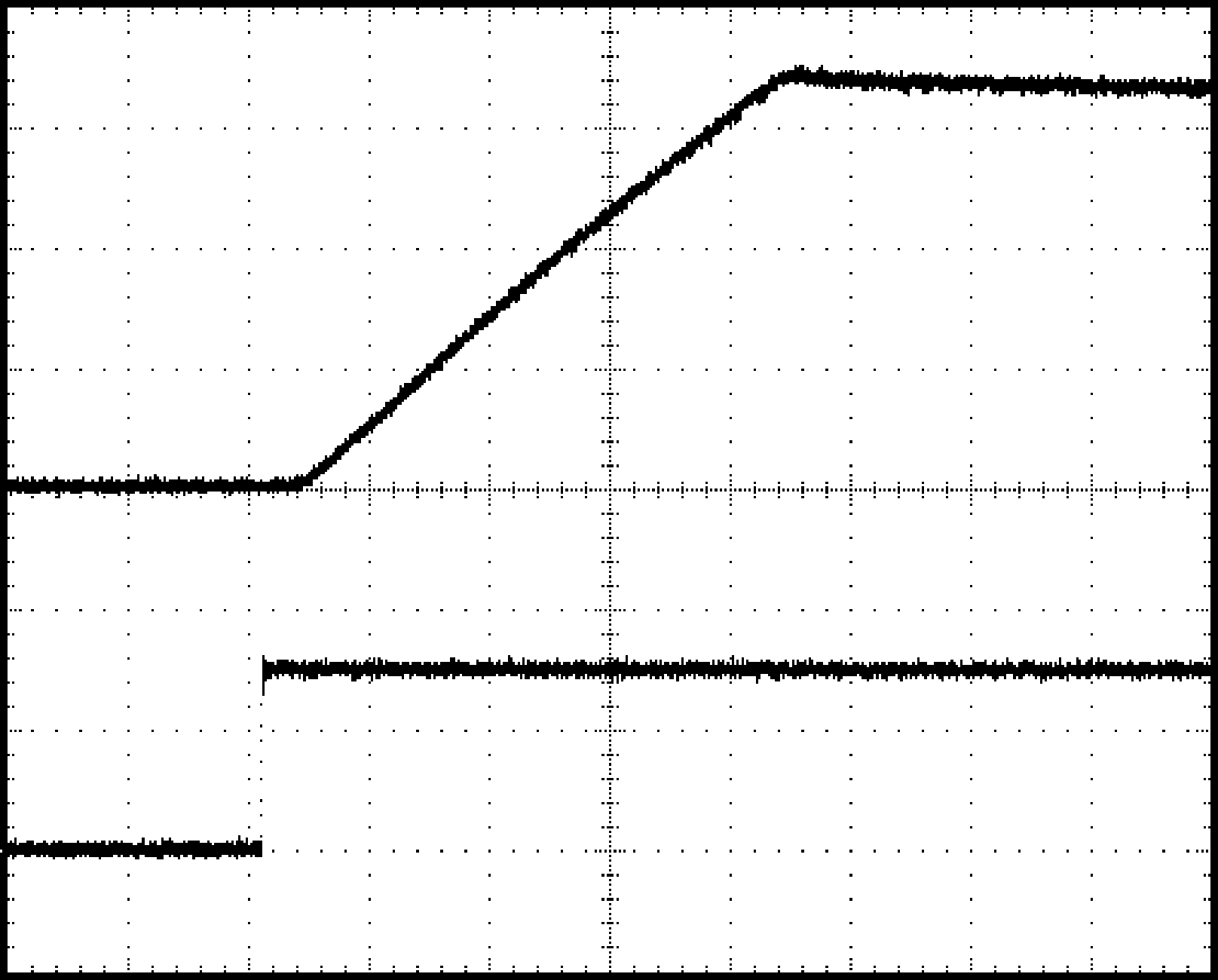
LM2840 LM2841 LM2842 30036772.png
VIN = 12 V IOUT = 50 mA
VOUT = 3.3 V Top trace: VOUT, 1V/div, DC-Coupled
T = 40 µs/div Bottom trace: SHDN, 2V/div, DC-Coupled
Figure 12. Start-Up Waveform
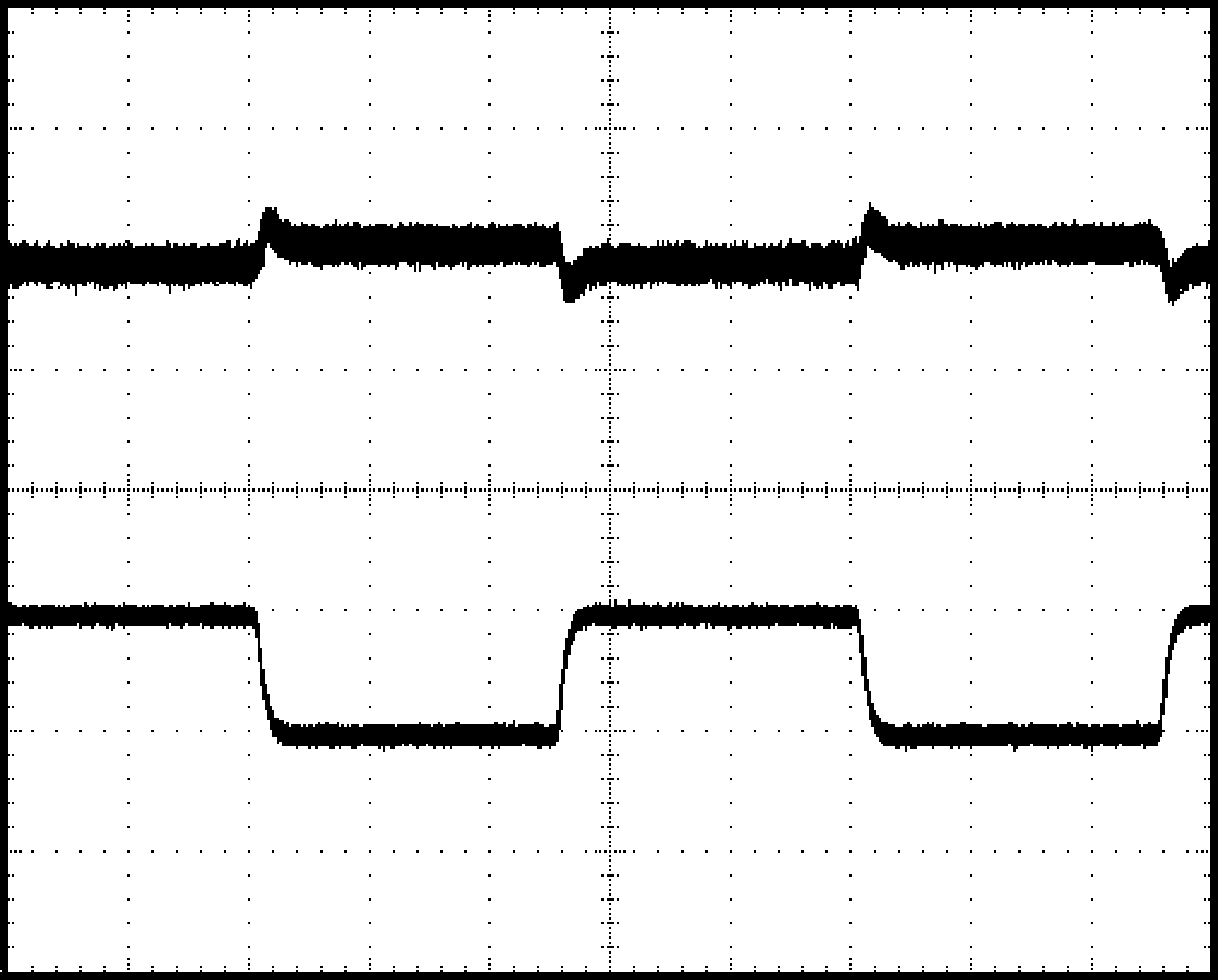
LM2840 LM2841 LM2842 30036771.png
VIN = 12 V IOUT = 300 mA to 200 mA to 300 mA
VOUT = 3.3 V Top trace: VOUT, 20 mV/div, AC-Coupled
T = 200 µs/div Bottom trace: IOUT, 100 mA/div, DC-Coupled
Figure 11. Load Transient Waveforms