SNOSBT3J January 2000 – March 2022 LM158-N , LM258-N , LM2904-N , LM358-N
PRODUCTION DATA
- 1 Features
- 2 Applications
- 3 Description
- 4 Revision History
- 5 Pin Configuration and Functions
- 6 Specifications
- 7 Detailed Description
- 8 Application and Implementation
- 9 Power Supply Recommendations
- 10Layout
- 11Device and Documentation Support
- 12Mechanical, Packaging, and Orderable Information
Package Options
Mechanical Data (Package|Pins)
Thermal pad, mechanical data (Package|Pins)
Orderable Information
5 Pin Configuration and Functions
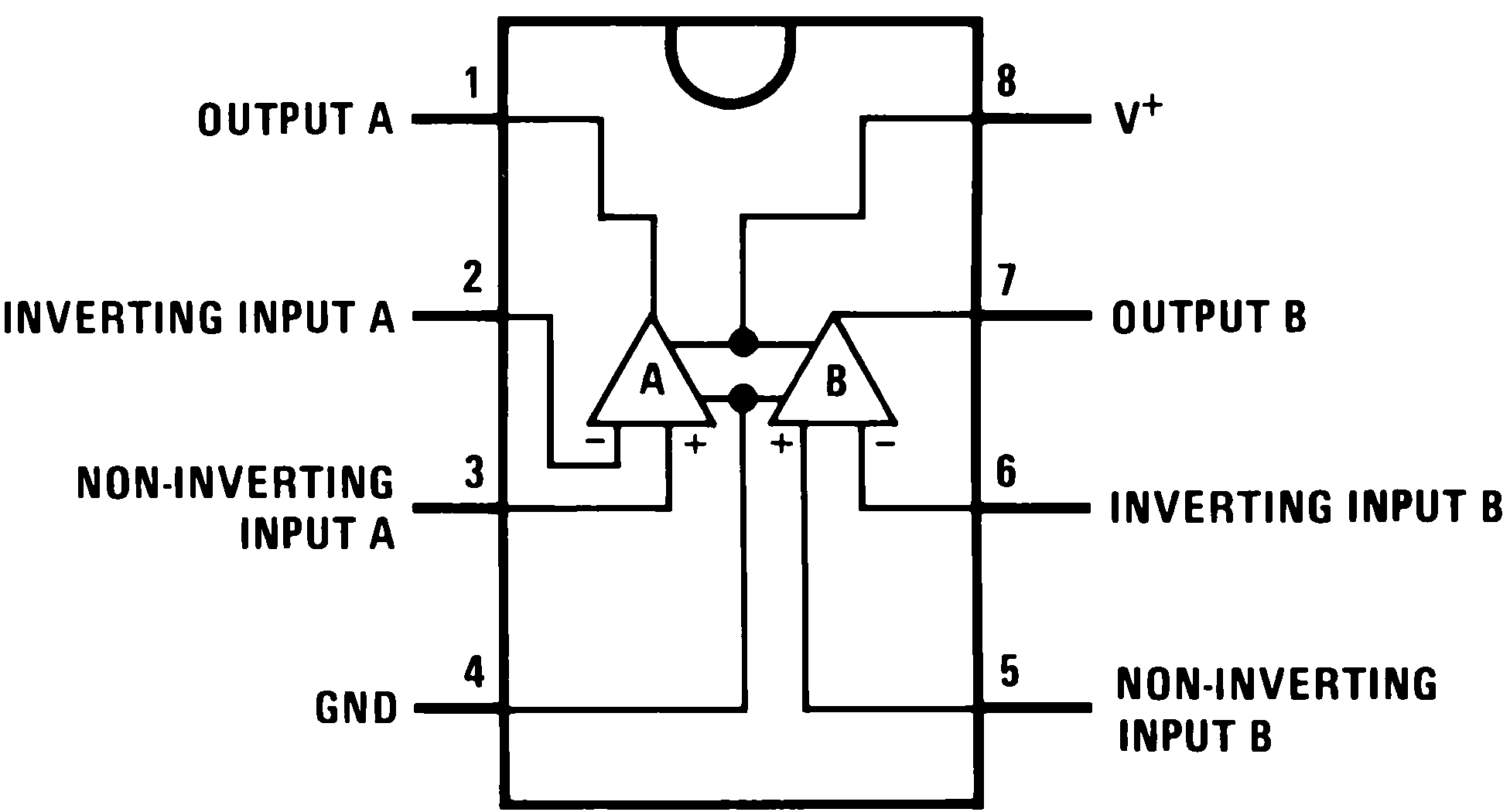
 Figure 5-1 D, P,
and NAB Package8-Pin SOIC, PDIP, and CDIP(Top View)
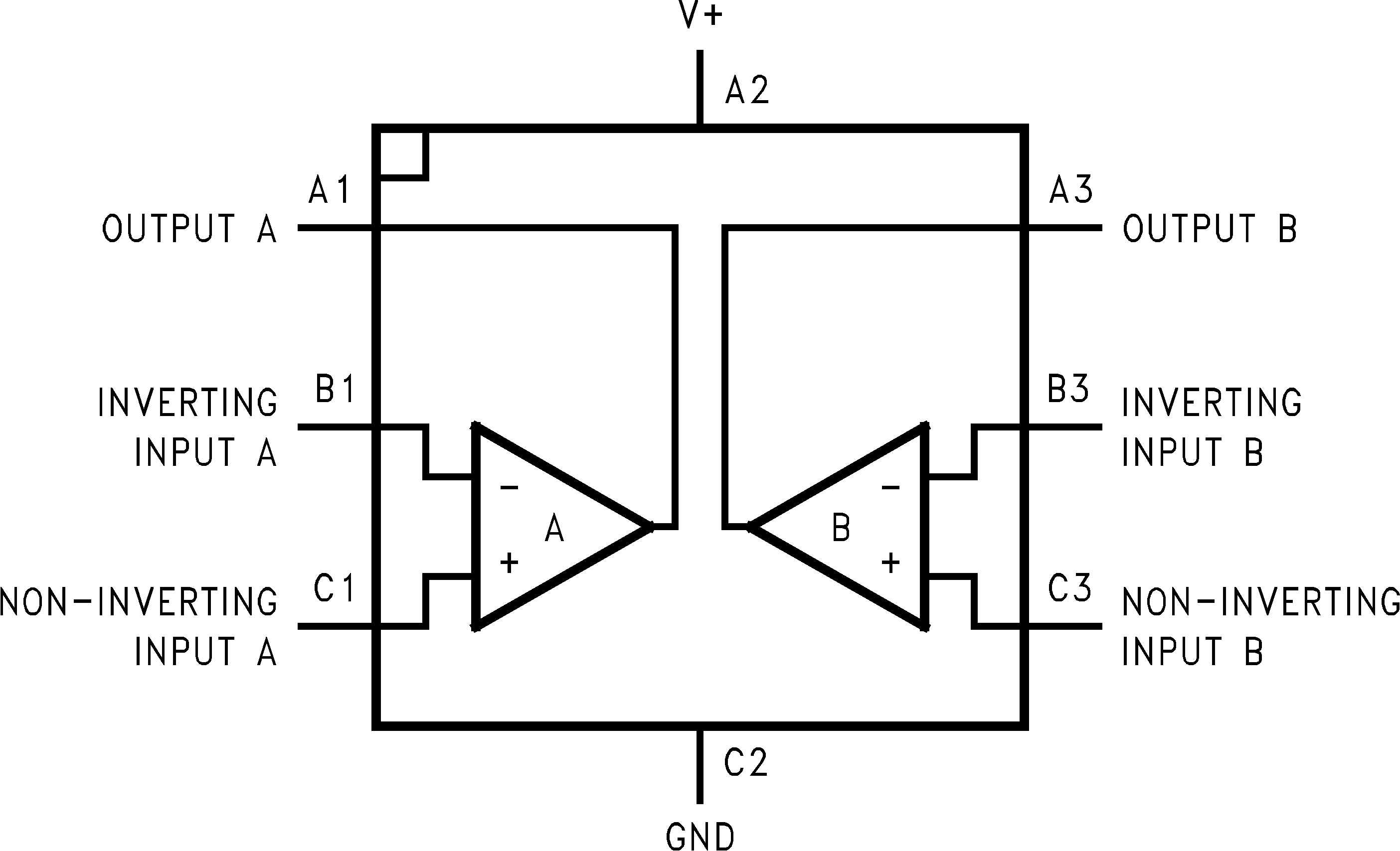
 Figure 5-3 YPB
Package8-Pin DSBGA
Top View
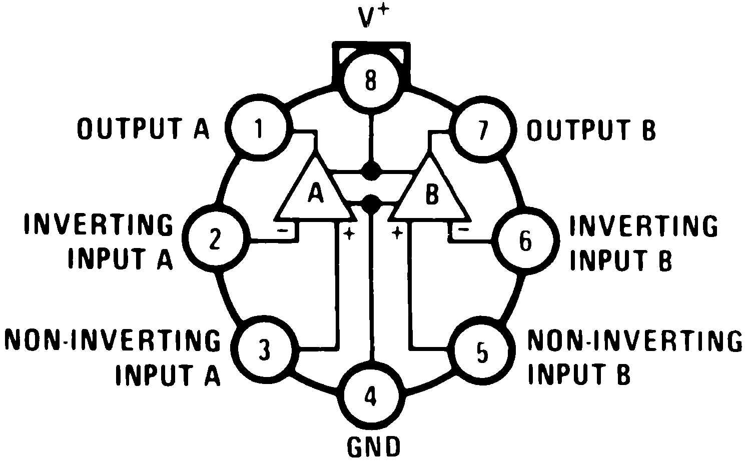
 Figure 5-2 LMC
Package8-Pin TO-99Top View
Figure 5-2 LMC
Package8-Pin TO-99Top ViewTable 5-1 Pin Functions
| PIN | TYPE(1) | DESCRIPTION | ||
|---|---|---|---|---|
| NAME | D/P/LMC | YPB | ||
| OUTA | 1 | A1 | O | Output, channel A |
| –INA | 2 | B1 | I | Inverting input, channel A |
| +INA | 3 | C1 | I | Non-inverting input, channel A |
| GND / V– | 4 | C2 | P | Ground for single-supply configurations. Negative supply for dual-supply configurations. |
| +INB | 5 | C3 | I | Non-inverting input, channel B |
| –INB | 6 | B3 | I | Inverting input, channel B |
| OUTB | 7 | A3 | O | Output, channel B |
| V+ | 8 | A2 | P | Positive supply |
(1) Signal Types: I = Input, O = Output, I/O
= Input or Output, P = Power