SNOSC48O June 2000 – December 2014 LM2936
PRODUCTION DATA.
- 1 Features
- 2 Applications
- 3 Description
- 4 Revision History
- 5 Pin Configuration and Functions
- 6 Specifications
- 7 Detailed Description
- 8 Application and Implementation
- 9 Power Supply Recommendations
- 10Layout
- 11Device and Documentation Support
- 12Mechanical, Packaging, and Orderable Information
Package Options
Mechanical Data (Package|Pins)
Thermal pad, mechanical data (Package|Pins)
- DCY|4
Orderable Information
7 Detailed Description
7.1 Overview
The LM2936 ultra-low quiescent current regulator features low dropout voltage and low current in the standby mode. With less than 15 μA quiescent current at a 100-μA load, the LM2936 is ideally suited for automotive and other battery operated systems. The LM2936 retains all of the features that are common to low dropout regulators including a low dropout PNP pass device, short circuit protection, reverse battery input protection, and thermal shutdown. The LM2936 has a 40-V maximum operating voltage limit, a −40°C to 125°C operating temperature range, and ±3% output voltage tolerance over the entire output current, input voltage, and temperature range.
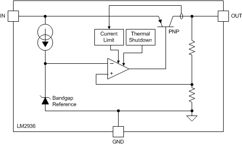
7.2 Functional Block Diagram
7.3 Feature Description
7.3.1 High Input Operating Voltage
Unlike namy other PNP low dropout regulators, the LM2936 remains fully operational with VIN = 40 V, and the LM2936HV remains fully operational with VIN = 60 V . Owing to power dissipation characteristics of the available packages, full output current cannot be ensured for all combinations of ambient temperature and input voltage.
While the LM2936HV maintains regulation to 60 V, it will not withstand a short circuit to ground on the output when VIN is above 40 V because of safe operating area limitations in the internal PNP pass device. Above 60V the LM2936 will break down with catastrophic effects on the regulator and possibly the load as well. Do not use this device in a design where the input operating voltage may exceed 40 V, or where transients are likely to exceed 60 V.
7.3.2 Thermal Shutdown (TSD)
The TSD circuitry of the LM2936 has been designed to protect the device against temporary thermal overload conditions. The TSD circuitry is not intended to replace proper heat-sinking. Continuously running the LM2936 device at TSD may degrade device reliability as the junction temperature will be exceeding the absolute maximum junction temperature rating. If the LM2936 goes into TSD mode, the output current will be shut off until the junction temperature falls approximately 10°C, then the output current will automatically be restored. The LM2936 will continuously cycle in and out of TSD until the condition is corrected. The LM2936 TSD junction temperature is typically 160°C.
7.3.3 Short-Circuit Current Limit
The output current limiting circuitry of the LM2936 has been designed to limit the output current in cases where the load impedance is unusually low. This includes situations where the output may be shorted directly to ground. Continuous operation of the LM2936 at the current limit will typically result in the LM2936 transitioning into TSD mode.
7.3.4 Shutdown (SD) Pin
The LM2936BM has a pin for shutting down the regulator output. Applying a Logic Level High (> 2 V) to the SD pin will cause the output to turn off. Leaving the SD pin open, connecting it to Ground, or applying a Logic Level Low (< 0.6 V) will allow the regulator output to turn on.
7.4 Device Functional Modes
The LM2936 design does not include any undervoltage lockout (UVLO), or overvoltage shutdown (OVSD) functions. Generally, the output voltage will track the input voltage until the input voltage is greater than VOUT + 1 V. When the input voltage is greater than VOUT + 1 V the LM2936 will be in linear operation, and the output voltage will be regulated; however, the device will be sensitive to any small perturbation of the input voltage. Device dynamic performance is improved when the input voltage is at least 2 V greater than the output voltage.