SLCS007K September 1973 – March 2017 LM111 , LM211 , LM311
PRODUCTION DATA.
- 1 Features
- 2 Applications
- 3 Description
- 4 Revision History
- 5 Pin Configuration and Functions
- 6 Specifications
- 7 Parameter Measurement Information
- 8 Detailed Description
- 9 Application and Implementation
- 10Power Supply Recommendations
- 11Layout
- 12Device and Documentation Support
- 13Mechanical, Packaging, and Orderable Information
Package Options
Refer to the PDF data sheet for device specific package drawings
Mechanical Data (Package|Pins)
- D|8
- P|8
- PS|8
- PW|8
Thermal pad, mechanical data (Package|Pins)
- PS|8
Orderable Information
6 Specifications
6.1 Absolute Maximum Ratings
over operating free-air temperature range (unless otherwise noted)(1)| MIN | MAX | UNIT | |||
|---|---|---|---|---|---|
| Supply voltage | VCC+(2) | 18 | V | ||
| VCC–(2) | –18 | ||||
| VCC+ – VCC– | 36 | ||||
| VID | Differential input voltage(3) | ±30 | V | ||
| VI | Input voltage (either input)(2)(4) | ±15 | V | ||
| Voltage from emitter output to VCC– | 30 | V | |||
| Voltage from collector output to VCC– | LM111 | 50 | V | ||
| LM211 | 50 | ||||
| LM211Q | 50 | ||||
| LM311 | 40 | ||||
| Duration of output short circuit to ground | 10 | s | |||
| TJ | Operating virtual-junction temperature | 150 | °C | ||
| Case temperature for 60 s | FK package | 260 | °C | ||
| Lead temperature 1,6 mm (1/16 inch) from case, 10 s | JG package | 300 | °C | ||
| Lead temperature 1,6 mm (1/16 inch) from case, 60 s | D, P, PS, or PW package | 260 | °C | ||
| Tstg | Storage temperature | −65 | 150 | °C | |
(1) Stresses beyond those listed under Absolute Maximum Ratings may cause permanent damage to the device. These are stress ratings only, and functional operation of the device at these or any other conditions beyond those indicated under Recommended Operating Conditions is not implied. Exposure to absolute-maximum-rated conditions for extended periods may affect device reliability.
(2) All voltage values, unless otherwise noted, are with respect to the midpoint between VCC+ and VCC–.
(3) Differential voltages are at IN+ with respect to IN–.
(4) The magnitude of the input voltage must never exceed the magnitude of the supply voltage or ±15 V, whichever is less.
6.2 ESD Ratings
| VALUE | UNIT | |||
|---|---|---|---|---|
| V(ESD) | Electrostatic discharge | Human body model (HBM), per ANSI/ESDA/JEDEC JS-001(1) | ±500 | V |
| Charged-device model (CDM), per JEDEC specification JESD22-C101(2) | ±750 | |||
(1) JEDEC document JEP155 states that 500-V HBM allows safe manufacturing with a standard ESD control process.
(2) JEDEC document JEP157 states that 250-V CDM allows safe manufacturing with a standard ESD control process.
6.3 Recommended Operating Conditions
| MIN | MAX | UNIT | |||
|---|---|---|---|---|---|
| VCC+ – VCC– | Supply voltage | 3.5 | 30 | V | |
| VI | Input voltage (|VCC+| ≤ 15 V) | VCC– + 0.5 | VCC+ – 1.5 | V | |
| TA | Operating free-air temperature range | LM111 | –55 | 125 | °C |
| LM211 | –40 | 85 | |||
| LM211Q | –40 | 125 | |||
| LM311 | 0 | 70 | |||
6.4 Thermal Information (8-Pin Packages)
| THERMAL METRIC(1) | LM211, LM311 | LM311 | LM111 | UNIT | |||
|---|---|---|---|---|---|---|---|
| D (SOIC) | P (PDIP) | PW (TSSOP) | PS (SO) | JG (CDIP) | |||
| 8 PINS | 8 PINS | 8 PINS | 8 PINS | 8 PINS | |||
| RθJA | Junction-to-ambient thermal resistance | 114.3 | 57.5 | 162 | 121.8 | — | °C/W |
| RθJC(top) | Junction-to-case (top) thermal resistance | 60.7 | 47.3 | 44.6 | 81.6 | 14.5 | °C/W |
| RθJB | Junction-to-board thermal resistance | 54.5 | 34.6 | 93 | 66.5 | — | °C/W |
| ψJT | Junction-to-top characterization parameter | 17.4 | 24.9 | 2.6 | 31.4 | — | °C/W |
| ψJB | Junction-to-board characterization parameter | 54 | 34.5 | 90.8 | 65.8 | — | °C/W |
(1) For more information about traditional and new thermal metrics, see the Semiconductor and IC Package Thermal Metrics application report.
6.5 Thermal Information (20-Pin Package)
| THERMAL METRIC(1) | LM111 | UNIT | |
|---|---|---|---|
| FK (LCCC) | |||
| 20 PINS | |||
| RθJC(top) | Junction-to-case (top) thermal resistance | 5.61 | °C/W |
(1) For more information about traditional and new thermal metrics, see the Semiconductor and IC Package Thermal Metrics application report.
6.6 Electrical Characteristics
at specified free-air temperature, VCC± = ±15 V (unless otherwise noted)| PARAMETER | TEST CONDITIONS | TA(1) | LM111 LM211 LM211Q |
LM311 | UNIT | ||||||
|---|---|---|---|---|---|---|---|---|---|---|---|
| MIN | TYP(2) | MAX | MIN | TYP(2) | MAX | ||||||
| VIO | Input offset voltage | See(3) | 25°C | 0.7 | 3 | 2 | 7.5 | mV | |||
| Full range | 4 | 10 | |||||||||
| IIO | Input offset current | See(3) | 25°C | 4 | 10 | 6 | 50 | nA | |||
| Full range | 20 | 70 | |||||||||
| IIB | Input bias current | 1 V ≤ VO ≤ 14 V | 25°C | 75 | 100 | 100 | 250 | nA | |||
| Full range | 150 | 300 | |||||||||
| IIL(S) | Low-level strobe current(4) |
V(strobe) = 0.3 V, VID ≤ –10 mV |
25°C | –3 | –3 | mA | |||||
| VICR | Common-mode input-voltage range(3) |
Lower range | Full range | –14.7 | –14.5 | –14.7 | –14.5 | V | |||
| Upper range | 13 | 13.8 | 13 | 13.8 | |||||||
| AVD | Large-signal differential-voltage amplification |
5 V ≤ VO ≤ 35 V, RL = 1 kΩ | 25°C | 40 | 200 | 40 | 200 | V/mV | |||
| IOH | High-level (collector) output leakage current |
I(strobe) = –3 mA, VID = 5 mV |
VOH = 35 V | 25°C | 0.2 | 10 | nA | ||||
| Full range | 0.5 | μA | |||||||||
| VID = 5 mV, VOH = 35 V | 25°C | 0.2 | 50 | nA | |||||||
| VOL | Low-level (collector-to-emitter) output voltage |
IOL = 50 mA | VID = –5 mV | 25°C | 0.75 | 1.5 | V | ||||
| VID = –10 mV | 25°C | 0.75 | 1.5 | ||||||||
| VCC+ = 4.5 V, VCC– = 0 V, IOL = 8 mA |
VID = –6 mV | Full range | 0.23 | 0.4 | |||||||
| VID = –10 mV | Full range | 0.23 | 0.4 | ||||||||
| ICC+ | Supply current from VCC+
output low |
VID = –10 mV, | No load | 25°C | 5.1 | 6 | 5.1 | 7.5 | mA | ||
| ICC– | Supply current from VCC–
output high |
VID = 10 mV, | No load | 25°C | –4.1 | –5 | –4.1 | –5 | mA | ||
(1) Unless otherwise noted, all characteristics are measured with BALANCE and BAL/STRB open and EMIT OUT grounded. Full range for LM111 is –55°C to 125°C, for LM211 is –40°C to 85°C, for LM211Q is –40°C to 125°C, and for LM311 is 0°C to 70°C.
(2) All typical values are at TA = 25°C.
(3) The offset voltages and offset currents given are the maximum values required to drive the collector output up to 14 V or down to 1 V with a pullup resistor of 7.5 kΩ to VCC+. These parameters actually define an error band and take into account the worst-case effects of voltage gain and input impedance.
6.7 Switching Characteristics
VCC± = ±15 V, TA = 25°C| PARAMETER | TEST CONDITIONS | LM111 LM211 LM211Q LM311 |
UNIT |
|---|---|---|---|
| TYP | |||
| Response time, low-to-high-level outputSee(1) | RC = 500 Ω to 5 V, CL = 5 pF, see (2) | 115 | ns |
| Response time, high-to-low-level outputSee(1) | 165 | ns |
(1) The response time specified is for a 100-mV input step with 5-mV overdrive and is the interval between the input step function and the instant when the output crosses 1.4 V.
(2) The package thermal impedance is calculated in accordance with MIL-STD-883.
6.8 Typical Characteristics
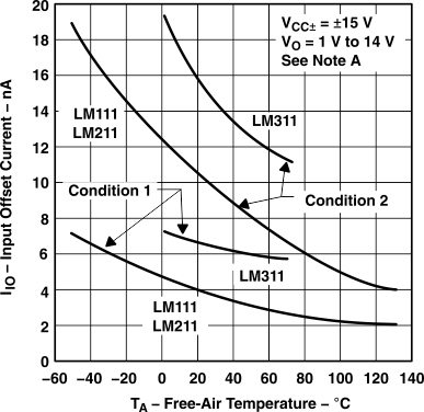
a.
Figure 1. Input Offset Current vs Free-Air Temperature
| Condition 1 is with BALANCE and BAL/STRB open. | ||
| Condition 2 is with BALANCE and BAL/STRB connected to VCC+. |
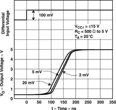 Figure 3. Output Response for Various Input Overdrives
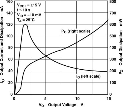 Figure 5. Output Current and Dissipation vs Output Voltage
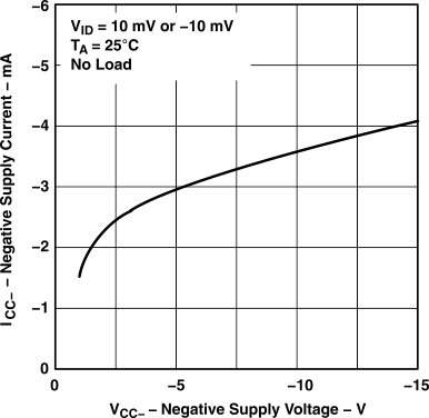 Figure 7. Negative Supply Current vs Negative Supply Voltage
a.
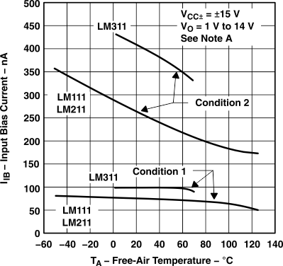
Figure 2. Input Bias Current vs Free-Air Temperature
| Condition 1 is with BALANCE and BAL/STRB open. | ||
| Condition 2 is with BALANCE and BAL/STRB connected to VCC+. |
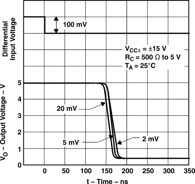 Figure 4. Output Response for Various Input Overdrives
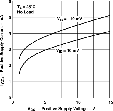 Figure 6. Positive Supply Current vs Positive Supply Voltage
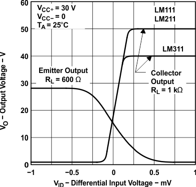 Figure 8. Voltage Transfer Characteristics and Test Circuits