SNVSAC2A March 2015 – June 2020 LM317A
PRODUCTION DATA.
- 1 Features
- 2 Applications
- 3 Description
- 4 Device Comparison Table
- 5 Pin Configuration and Functions
- 6 Specifications
- 7 Detailed Description
-
8 Application and Implementation
- 8.1 Application Information
- 8.2
Typical Applications
- 8.2.1 1.25-V to 25-V Adjustable Regulator
- 8.2.2 5-V Logic Regulator With Electronic Shutdown
- 8.2.3 Slow Turnon 15-V Regulator
- 8.2.4 Adjustable Regulator With Improved Ripple Rejection
- 8.2.5 High-Stability 10-V Regulator
- 8.2.6 High-Current Adjustable Regulator
- 8.2.7 Emitter-Follower Current Amplifier
- 8.2.8 1-A Current Regulator
- 8.2.9 Common-Emitter Amplifier
- 8.2.10 Low-Cost 3-A Switching Regulator
- 8.2.11 Current-Limited Voltage Regulator
- 8.2.12 Adjusting Multiple On-Card Regulators With Single Control
- 8.2.13 AC Voltage Regulator
- 8.2.14 12-V Battery Charger
- 8.2.15 Adjustable 4-A Regulator
- 8.2.16 Current-Limited 6-V Charger
- 8.2.17 Digitally-Selected Outputs
- 9 Power Supply Recommendations
- 10Layout
- 11Device and Documentation Support
- 12Mechanical, Packaging, and Orderable Information
Package Options
Mechanical Data (Package|Pins)
Thermal pad, mechanical data (Package|Pins)
- DCY|4
Orderable Information
7.3.1 Load Regulation
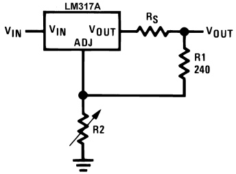
The LM317A is capable of providing extremely good load regulation but a few precautions are needed to obtain maximum performance. The current set resistor, R1, should be connected near the output terminal of the regulator rather than near the load. If R1 is placed too far from the output terminal, then the increased trace resistance, RS, will cause an error voltage drop in the adjustment loop and degrade load regulation performance. Therefore, R1 should be placed as close as possible to the output terminal to minimize RS and maximize load regulation performance.
Figure 16 shows the effect of the trace resistance, RS, when R1 is placed far from the output terminal of the regulator. It is clear that RS will cause an error voltage drop especially during higher current loads, so it is important to minimize the RS trace resistance by keeping R1 close to the regulator output terminal.
 Figure 16. Regulator with Line Resistance in Output Lead
 With the TO package, care should be taken to minimize the wire length of the output lead. The ground of R2 can be returned near the ground of the load to provide remote ground sensing and improve load regulation.