SNVS773D April 2000 – September 2015 LM317HV
PRODUCTION DATA.
- 1 Features
- 2 Applications
- 3 Description
- 4 Revision History
- 5 Device Comparison Table
- 6 Pin Configuration and Functions
- 7 Specifications
- 8 Detailed Description
-
9 Application and Implementation
- 9.1 Application Information
- 9.2
Typical Applications
- 9.2.1 1.25-V to 45-V High Voltage Adjustable Regulator
- 9.2.2 Digitally Selected Outputs
- 9.2.3 Logic Regulator (5-V) With Electronic Shutdown
- 9.2.4 Slow Turnon 15-V Regulator
- 9.2.5 Adjustable Regulator With Improved Ripple Rejection
- 9.2.6 High Stability 10-V Regulator
- 9.2.7 High Current Adjustable Regulator
- 9.2.8 Emitter Follower Current Amplifier
- 9.2.9 1-A Current Regulator
- 9.2.10 Common Emitter Amplifier
- 9.2.11 Low-Cost, 3-A Switching Regulator
- 9.2.12 Adjustable Multiple On-Card Regulators With Single Control
- 9.2.13 AC Voltage Regulator
- 9.2.14 12-V Battery Charger
- 9.2.15 Adjustable 4-A Regulator
- 9.2.16 Current Limited 6-V Charger
- 10Power Supply Recommendations
- 11Layout
- 12Device and Documentation Support
- 13Mechanical, Packaging, and Orderable Information
Package Options
Mechanical Data (Package|Pins)
- NDE|3
Thermal pad, mechanical data (Package|Pins)
Orderable Information
11 Layout
11.1 Layout Guidelines
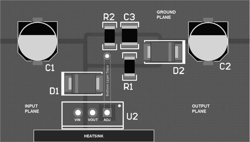
Some layout guidelines should be followed to ensure proper regulation of the output voltage with minimum noise. Traces carrying the load current should be wide to reduce the amount of parasitic trace inductance and the feedback loop from V2 to ADJ should be kept as short as possible. To improve PSRR, a bypass capacitor can be placed at the ADJ pin and should be located as close as possible to the IC. In cases when VIN shorts to ground, an external diode should be placed from VOUT to VIN to divert the surge current from the output capacitor and protect the IC. Similarly, in cases when a large bypass capacitor is placed at the ADJ pin and VOUT shorts to ground, an external diode should be placed from ADJ to VOUT to provide a path for the bypass capacitor to discharge. These diodes should be placed close to the corresponding IC pins to increase their effectiveness.
11.2 Layout Example
 Figure 33. Layout Example (TO-220 Package)