SNOS935C February 2001 – December 2014 LM321
PRODUCTION DATA.
- 1 Features
- 2 Applications
- 3 Description
- 4 Revision History
- 5 Pin Configuration and Functions
- 6 Specifications
- 7 Detailed Description
- 8 Application and Implementation
- 9 Power Supply Recommendations
- 10Layout
- 11Device and Documentation Support
- 12Mechanical, Packaging, and Orderable Information
Package Options
Mechanical Data (Package|Pins)
- DBV|5
Thermal pad, mechanical data (Package|Pins)
Orderable Information
6 Specifications
6.1 Absolute Maximum Ratings (1)
| MIN | MAX | UNIT | |
|---|---|---|---|
| Differential Input Voltage | ±Supply Voltage | ||
| Input Current (VIN < −0.3 V) (2) | 50 | mA | |
| Supply Voltage (V+ - V−) | 32 | V | |
| Input Voltage | −0.3 | 32 | V |
| Output Short Circuit to GND, V+ ≤ 15 V and TA = 25°C (3) | Continuous | ||
| Junction Temperature (4) | 150 | °C | |
| Mounting Temperature: Lead temperature (Soldering, 10 sec) | 260 | °C | |
| Mounting Temperature: Infrared (10 sec) | 215 | °C | |
| Storage temperature, Tstg | –65 | 150 | °C |
(1) Stresses beyond those listed under Absolute Maximum Ratings may cause permanent damage to the device. These are stress ratings only, which do not imply functional operation of the device at these or any other conditions beyond those indicated under Recommended Operating Conditions. Exposure to absolute-maximum-rated conditions for extended periods may affect device reliability.
(2) This input current will only exist when the voltage at any of the input leads is driven negative. It is due to the collector base junction of the input PNP transistors becoming forward biased and thereby acting as input diode clamps. In addition to this diode action, there is also lateral NPN parasitic transistor action on the IC chip. This transistor action can cause the output voltages of the operational amplifer to go to the V+ voltage level (or to ground for a large overdrive) for the time duration that an input is driven negative. This is not destructive and normal output states will re-establish when the input voltage, which was negative, again returns to a value greater than −0.36V (at 25°C).
(3) Short circuits from the output V+ can cause excessive heating and eventual destruction. When considering short circuits to ground the maximum output current is approximately 40mA independent of the magnitude of V+. At values of supply voltage in excess of +15V, continuous short circuits can exceed the power dissipation ratings and cause eventual destruction.
(4) The maximum power dissipation is a function of TJ(MAX), θJA , and TA. The maximum allowable power dissipation at any ambient temperature is PD = (TJ(MAX) - TA)/ θJA. All numbers apply for packages soldered directly onto a PC board.
6.2 ESD Ratings
| VALUE | UNIT | |||
|---|---|---|---|---|
| V(ESD) | Electrostatic discharge | Human-body model (HBM), per ANSI/ESDA/JEDEC JS-001(1) | ±300 | V |
(1) JEDEC document JEP155 states that 500-V HBM allows safe manufacturing with a standard ESD control process.
6.3 Recommended Operating Conditions
| MIN | MAX | UNIT | |
|---|---|---|---|
| Temperature Range | −40 | 85 | °C |
| Supply Voltage | 3 | 30 | V |
6.4 Thermal Information
| THERMAL METRIC(1) | LM321 | UNIT | |
|---|---|---|---|
| DBV | |||
| 5 PINS | |||
| RθJA | Junction-to-ambient thermal resistance | 265 | °C/W |
(1) For more information about traditional and new thermal metrics, see the IC Package Thermal Metrics application report, SPRA953.
6.5 Electrical Characteristics
Unless otherwise specified, all limits specified for at TA = 25°C; V+ = 5 V, V− = 0 V, VO = 1.4 V| PARAMETER | TEST CONDITIONS | MIN | TYP | MAX | UNIT | ||
|---|---|---|---|---|---|---|---|
| VOS | Input Offset Voltage | (1) | 2 | 7 | mV | ||
| (1), –40°C ≤ TJ ≤ 85°C | 9 | ||||||
| IOS | Input Offset Current | 5 | 50 | nA | |||
| –40°C ≤ TJ ≤ 85°C | 150 | ||||||
| IB | Input Bias Current (2) | 45 | 250 | nA | |||
| –40°C ≤ TJ ≤ 85°C | 500 | ||||||
| VCM | Input Common-Mode Voltage Range | V+ = 30 V (3), for CMRR > = 50dB | 0 | V+ - 1.5 | V | ||
| V+ = 30 V (3), for CMRR > = 50dB, –40°C ≤ TJ ≤ 85°C | V+ - 2 | ||||||
| AV | Large Signal Voltage Gain | (V+ = 15 V, RL = 2kΩ, VO = 1.4 V to 11.4 V) | 25 | 100 | V/mV | ||
| (V+ = 15 V, RL = 2kΩ, VO = 1.4 V to 11.4 V), –40°C ≤ TJ ≤ 85°C | 15 | ||||||
| PSRR | Power Supply Rejection Ratio | RS ≤ 10kΩ, V+ ≤ 5 V to 30 V |
65 | 100 | dB | ||
| CMRR | Common Mode Rejection Ratio | RS ≤ 10kΩ | 65 | 85 | dB | ||
| VO | Output Swing | VOH | V+ = 30 V, RL = 2kΩ, –40°C ≤ TJ ≤ 85°C | 26 | V | ||
| V+ = 30 V, RL = 10kΩ, –40°C ≤ TJ ≤ 85°C | 27 | 28 | |||||
| VOL | V+ = 5 V, RL = 10kΩ, –40°C ≤ TJ ≤ 85°C | 5 | 20 | mV | |||
| IS | Supply Current, No Load | V+ = 5 V | 0.430 | 1.15 | mA | ||
| V+ = 5 V, –40°C ≤ TJ ≤ 85°C | 0.7 | 1.2 | |||||
| V+ = 30 V | 0.660 | 2.85 | |||||
| V+ = 30 V, –40°C ≤ TJ ≤ 85°C | 1.5 | 3 | |||||
| ISOURCE | Output Current Sourcing | VID = +1 V, V+ = 15 V, VO = 2 V | 20 | 40 | mA | ||
| VID = +1 V, V+ = 15 V, VO = 2 V, –40°C ≤ TJ ≤ 85°C | 10 | 20 | |||||
| ISINK | Output Current Sinking | VID = −1 V, V+ = 15 V, VO = 2 V | 10 | 20 | mA | ||
| VID = −1 V, V+ = 15 V, VO = 2 V, –40°C ≤ TJ ≤ 85°C | 5 | 8 | |||||
| VID = −1 V, V+ = 15 V, VO = 0.2 V | 12 | 100 | µA | ||||
| IO | Output Short Circuit to Ground (4) |
V+ = 15 V | 40 | 85 | mA | ||
| SR | Slew Rate | V+ = 15 V, RL = 2kΩ, VIN = 0.5 to 3 V, CL = 100pF, Unity Gain | 0.4 | V/µs | |||
| GBW | Gain Bandwidth Product | V+ = 30 V, f = 100kHz, VIN = 10 mV, RL =2kΩ, CL = 100 pF | 1 | MHz | |||
| φm | Phase Margin | 60 | degrees | ||||
| THD | Total Harmonic Distortion | f = 1kHz, AV = 20dB, RL = 2kΩ, VO = 2VPP, CL = 100 pF, V+ = 30 V | 0.015% | ||||
| en | Equivalent Input Noise Voltage | f = 1kHz, RS = 100Ω, V+ = 30 V | 40 | nV/√Hz | |||
(1) VO ≅ 1.4 V, RS = 0Ω with V+ from 5 V to 30 V; and over the full input common-mode range (0 V to V+ - 1.5 V) at 25°C.
(2) The direction of the input current is out of the IC due to the PNP input stage. This current is essentially constant, independent of the state of the output so no loading change exists on the input lines.
(3) The input common-mode voltage of either input signal voltage should not be allowed to go negative by more than 0.3 V (at 25°C). The upper end of the common-mode voltage range is V+ - 1.5 V at 25°C, but either or both inputs can go to +32 V without damage, independent of the magnitude of V+.
(4) Short circuits from the output V+ can cause excessive heating and eventual destruction. When considering short circuits to ground the maximum output current is approximately 40mA independent of the magnitude of V+. At values of supply voltage in excess of +15V, continuous short circuits can exceed the power dissipation ratings and cause eventual destruction.
6.6 Typical Characteristics
Unless otherwise specified, VS = 5 V, single supply, TA = 25°C.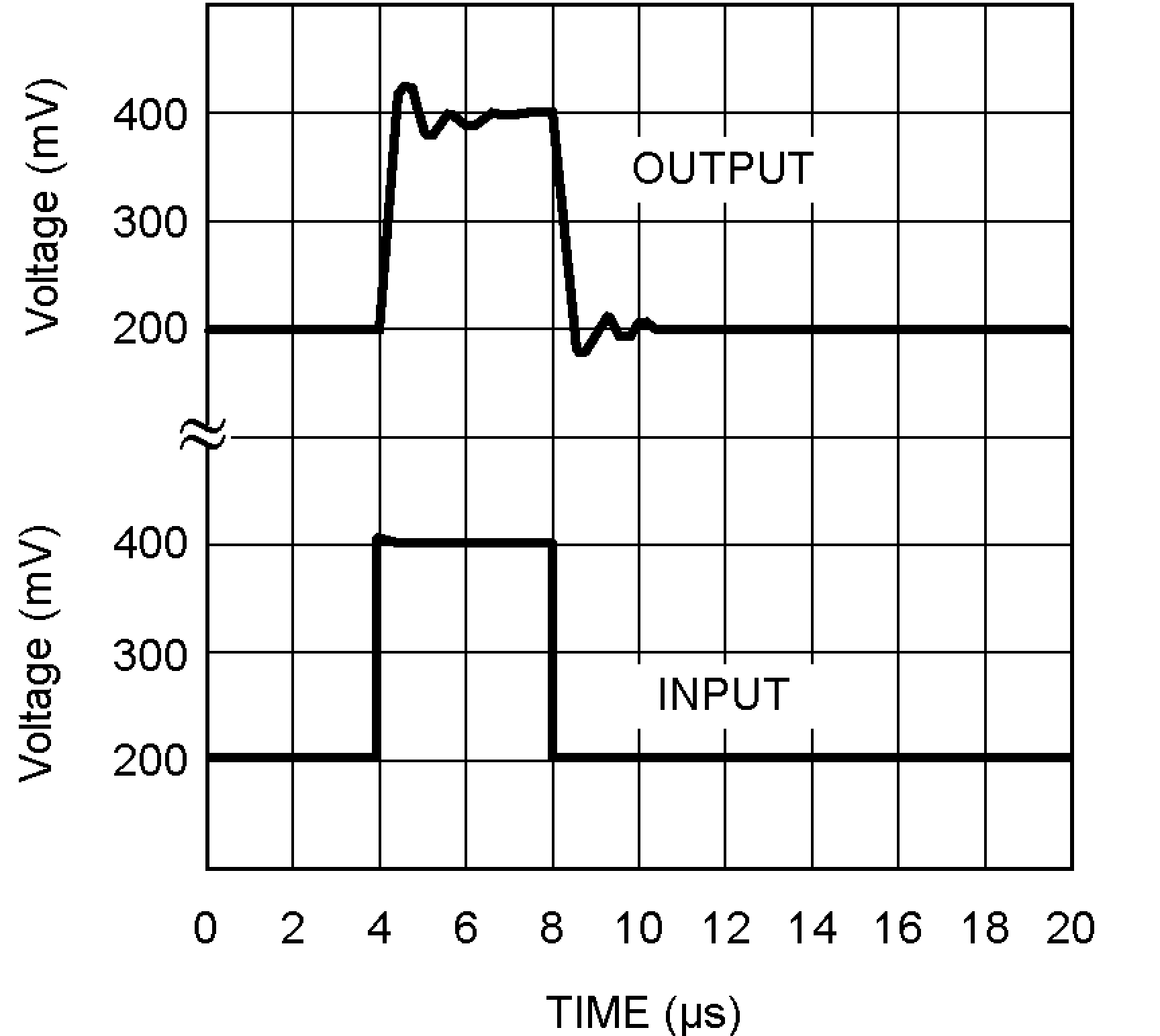 Figure 1. Small Signal Pulse Response
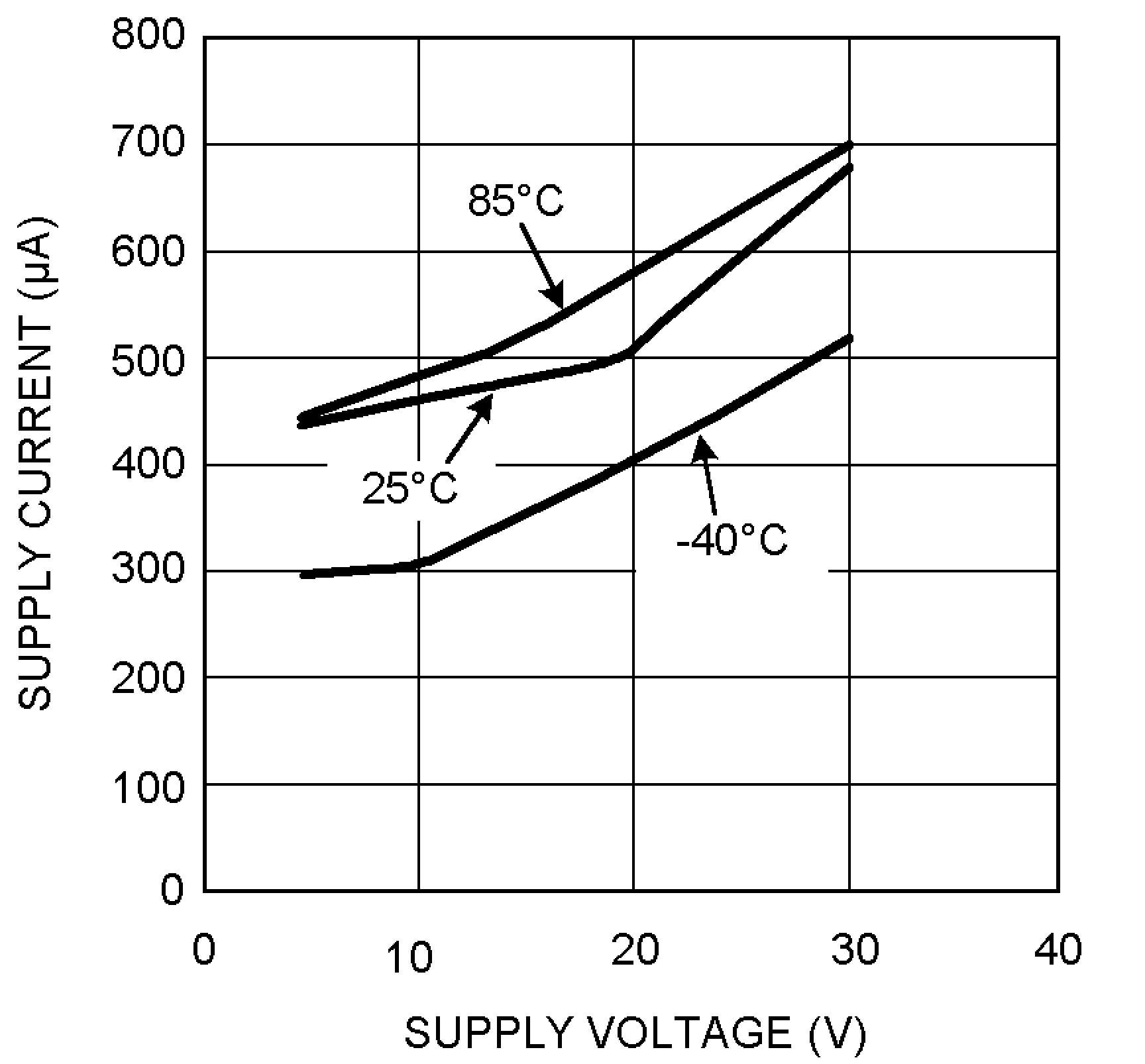 Figure 3. Supply Current vs. Supply Voltage
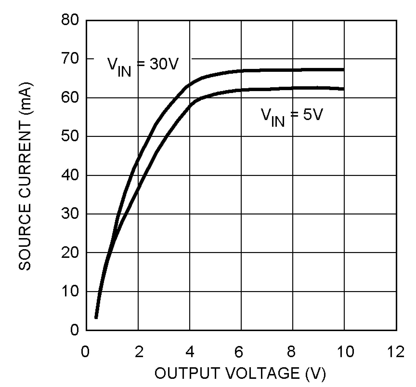 Figure 5. Source Current vs. Output Voltage
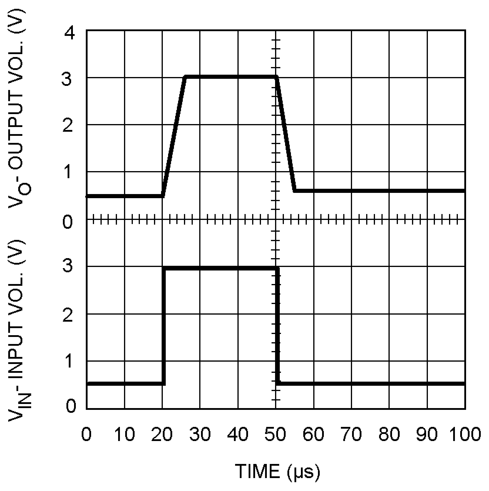 Figure 2. Large Signal Pulse Response
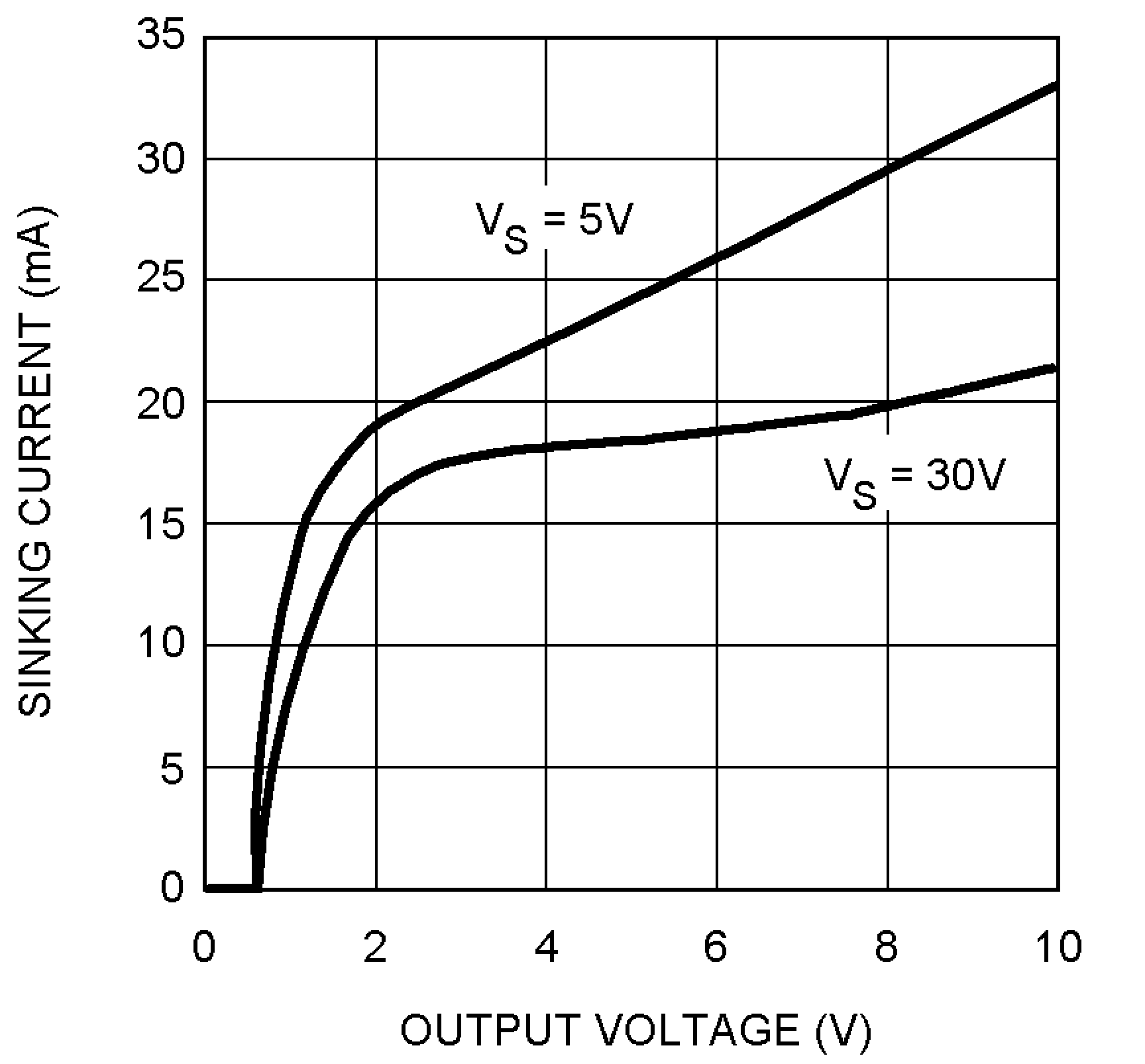 Figure 4. Sinking Current vs Output Voltage
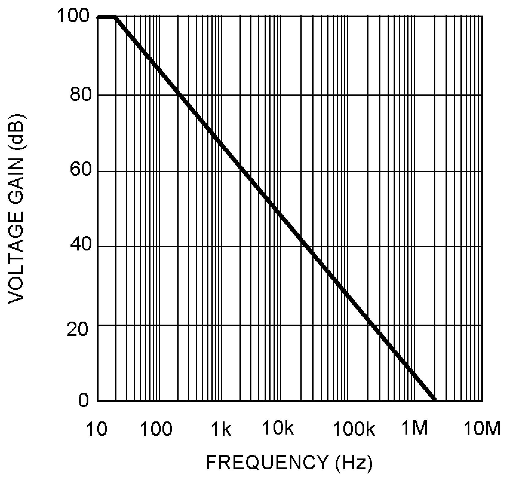 Figure 6. Open Loop Frequency Response