SNOSB38C January 2009 – November 2017 LM3241
PRODUCTION DATA.
- 1 Features
- 2 Applications
- 3 Description
- 4 Revision History
- 5 Pin Configuration and Functions
- 6 Specifications
- 7 Detailed Description
- 8 Application and Implementation
- 9 Power Supply Recommendations
- 10Layout
- 11Device and Documentation Support
- 12Mechanical, Packaging, and Orderable Information
Package Options
Mechanical Data (Package|Pins)
- YZR|6
Thermal pad, mechanical data (Package|Pins)
Orderable Information
1 Features
- 6-MHz (typ.) PWM Switching Frequency
- Operates from a Single Li-Ion Cell (2.7 V to 5.5 V)
- Adjustable Output Voltage (0.6 V to 3.4 V)
- 750-mA Maximum Load Capability
- High Efficiency (95% typ. at 3.9 VIN, 3.3 VOUT at 500 mA)
- Automatic Eco-mode™ and PWM Mode Change
- 6-Bump DSBGA Package
- Current Overload Protection
- Thermal Overload Protection
- Soft Start Function
- CIN and COUT are 0402 (1005) Case Size and 6.3 V of Rated-Voltage Ceramic Capacitor
- Small Chip Inductor in 0805 (2012) Case Size
2 Applications
- Battery-Powered 3G and 4G Power Amplifiers
- Hand-Held Radios
- RF PC Cards
- Battery-Powered RF Devices
3 Description
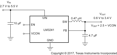
The LM3241 is a DC-DC converter optimized for powering RF power amplifiers (PAs) from a single Lithium-Ion cell. The device can also be used in many other applications. The device steps down an input voltage from 2.7 V to 5.5 V to an adjustable output voltage from 0.6 V to 3.4 V. The output voltage is set using a VCON analog input for controlling power levels and efficiency of the RF PA.
The LM3241 offers three modes of operation. In PWM mode the device operates at a fixed frequency of 6 MHz (typical) which minimizes RF interference when driving medium-to-heavy loads. At light-load conditions, the device enters into Eco-mode automatically and operates with reduced switching frequency. In Eco-mode, the quiescent current is reduced and extends the battery life. Shutdown mode turns the device off and reduces battery consumption to 0.1 µA (typical).
The LM3241 is available in a 6-bump lead-free DSBGA package. A high-switching frequency (6 MHz) allows use of tiny surface-mount components. Only three small external surface-mount components, an inductor and two ceramic capacitors are required.
Device Information(1)
| PART NUMBER | PACKAGE | BODY SIZE (NOM) |
|---|---|---|
| LM3241 | DSBGA (6) | 1.50 mm × 1.30 mm |
- For all available packages, see the orderable addendum at the end of the data sheet.
Typical Application
