SNOSBI2C June 1999 – September 2015 LM231 , LM331
PRODUCTION DATA.
- 1 Features
- 2 Applications
- 3 Description
- 4 Revision History
- 5 Description continued
- 6 Pin Configuration and Functions
- 7 Specifications
- 8 Detailed Description
- 9 Application and Implementation
- 10Power Supply Recommendations
- 11Layout
- 12Device and Documentation Support
- 13Mechanical, Packaging, and Orderable Information
Package Options
Mechanical Data (Package|Pins)
- P|8
Thermal pad, mechanical data (Package|Pins)
Orderable Information
9 Application and Implementation
NOTE
Information in the following applications sections is not part of the TI component specification, and TI does not warrant its accuracy or completeness. TI’s customers are responsible for determining suitability of components for their purposes. Customers should validate and test their design implementation to confirm system functionality.
9.1 Application Information
9.1.1 Simplified Voltage-to-Frequency Converter
The operation of these blocks is best understood by going through the operating cycle of the basic V-to-F converter, Figure 13, which consists of the simplified block diagram of the LMx31 and the various resistors and capacitors connected to it.
The voltage comparator compares a positive input voltage, V1, at pin 7 to the voltage, Vx, at pin 6. If V1 is greater, the comparator will trigger the 1-shot timer. The output of the timer will turn ON both the frequency output transistor and the switched current source for a period t = 1.1 RtCt. During this period, the current i will flow out of the switched current source and provide a fixed amount of charge, Q = i × t, into the capacitor, CL. This will normally charge Vx up to a higher level than V1. At the end of the timing period, the current i will turn OFF, and the timer will reset itself.
Now there is no current flowing from pin 1, and the capacitor CL will be gradually discharged by RL until Vx falls to the level of V1. Then the comparator will trigger the timer and start another cycle.
The current flowing into CL is exactly IAVE = i × (1.1×RtCt) × f, and the current flowing out of CL is exactly Vx/RL ≃ VIN/RL. If VIN is doubled, the frequency will double to maintain this balance. Even a simple V-to-F converter can provide a frequency precisely proportional to its input voltage over a wide range of frequencies.
9.1.2 Principles of Operation
The LMx31 are monolithic circuits designed for accuracy and versatile operation when applied as voltage-to-frequency (V-to-F) converters or as frequency-to-voltage (F-to-V) converters. A simplified block diagram of the LMx31 is shown in Figure 13 and consists of a switched current source, input comparator, and 1-shot timer.
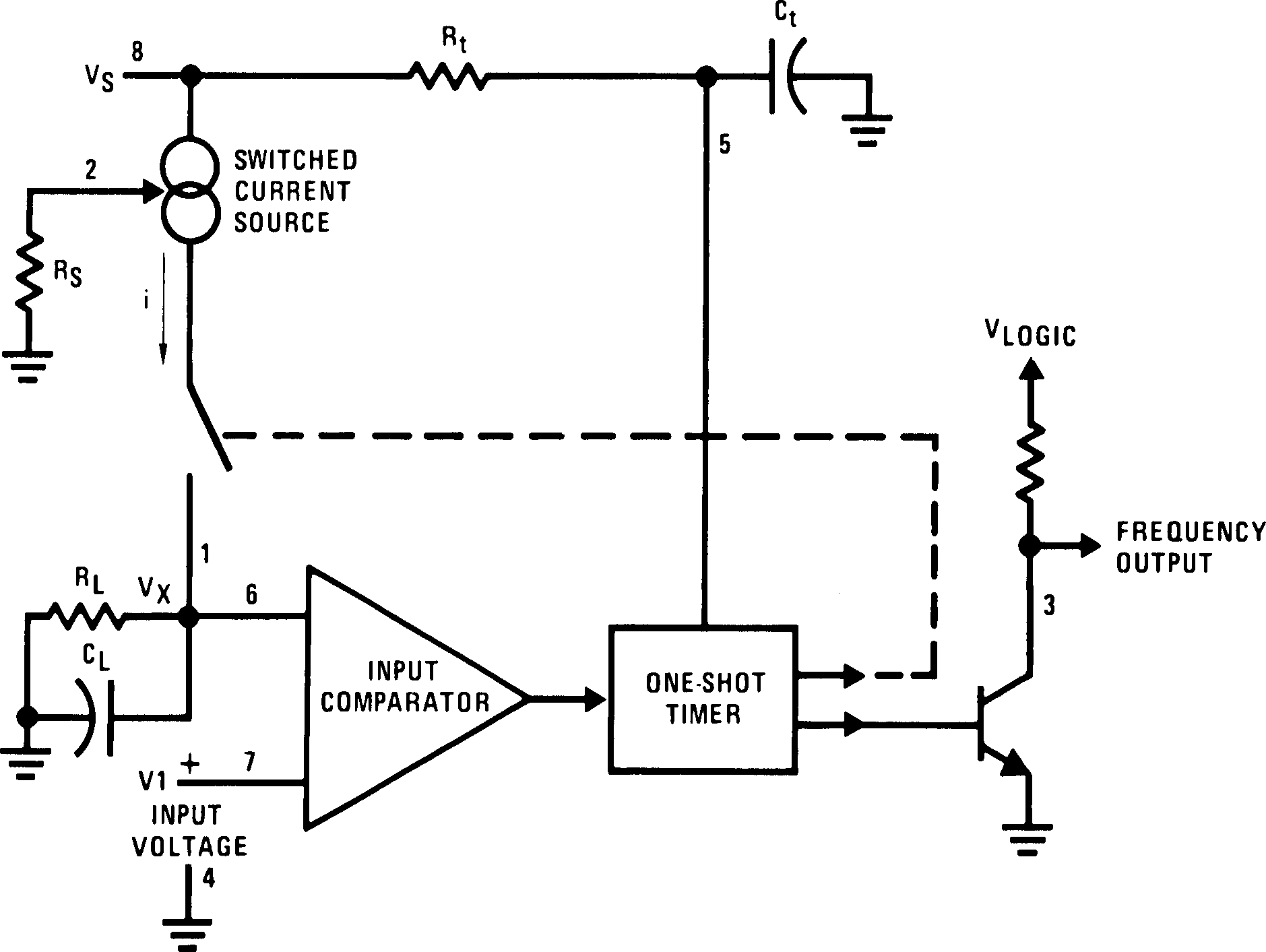 Figure 13. Simplified Block Diagram of Stand-Alone
Voltage-to-Frequency Converter and
External Components
9.2 Typical Applications
9.2.1 Basic Voltage-to-Frequency Converter
The simple stand-alone V-to-F converter shown in Figure 14 includes all the basic circuitry of Figure 13 plus a few components for improved performance.
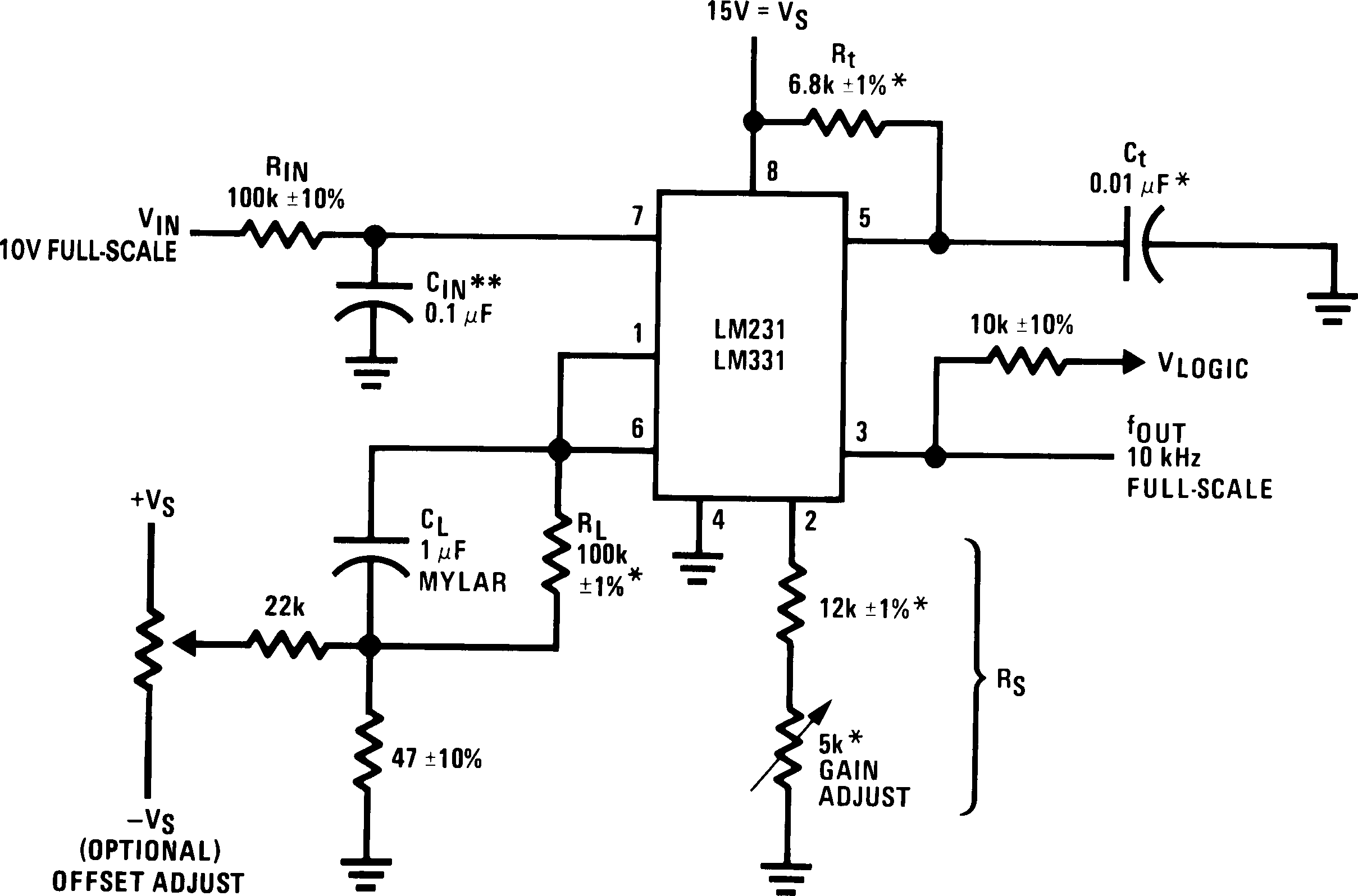

*Use stable components with low temperature coefficients. See Application Information.
**0.1 μF or 1 μF, See Typical Applications.
with ±0.03% Typical Linearity (f = 10 Hz to 11 kHz)
9.2.1.1 Design Requirements
For this example, the system requirements are 0.05% linearity over an output frequency range of 10 Hz to 4 kHz with an input voltage range of 25 mV to 12.5 V. The available supply voltage is 15.0 V.
9.2.1.2 Detailed Design Procedure
A capacitor CIN is added from pin 7 to ground to act as a filter for VIN, use of a 0.1 μF is appropriate for this application. A value of 0.01 μF to 0.1 μF will be adequate in most cases; however, in cases where better filtering is required, a 1-μF capacitor can be used. When the RC time constants are matched at pin 6 and pin 7, a voltage step at VIN will cause a step change in fOUT. If CIN is much less than CL, a step at VIN may cause fOUT to stop momentarily.
Next, we cancel the comparator bias current by setting RIN to 100 kΩ to match RL. This will help to minimize any frequency offset.
For best results, all the components should be stable low-temperature-coefficient components, such as metal-film resistors. The capacitor should have low dielectric absorption; depending on the temperature characteristics desired, NPO ceramic, polystyrene, Teflon or polypropylene are best suited.
The resistance RS at pin 2 is made up of a 12-kΩ fixed resistor plus a 5-kΩ (cermet, preferably) gain adjust rheostat. The function of this adjustment is to trim out the gain tolerance of the LMx31, and the tolerance of Rt, RL and Ct.
A 47-Ω resistor in series with the 1-μF capacitor (CL) provides hysteresis, which helps the input comparator provide the excellent linearity.
This results in the transfer function of ƒOUT = (VIN / 2.09 V) × (RS / RL) × (1 / RtCt).
9.2.1.3 Application Curve
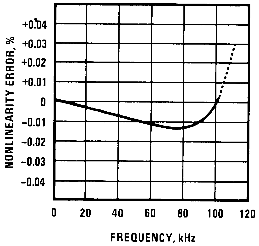 Figure 15. Output Non-Linearity Error vs. Frequency
9.2.2 Precision V-To-F Converter
In this circuit, integration is performed by using a conventional operational amplifier and feedback capacitor, CF. When the integrator's output crosses the nominal threshold level at pin 6 of the LMx31, the timing cycle is initiated.
The average current fed into the summing point of the op-amp (pin 2) is i × (1.1 RtCt) × f which is perfectly balanced with −VIN/RIN. In this circuit, the voltage offset of the LMx31 input comparator does not affect the offset or accuracy of the V-to-F converter as it does in the stand-alone V-to-F converter; nor does the LM231/331 bias current or offset current. Instead, the offset voltage and offset current of the operational amplifier are the only limits on how small the signal can be accurately converted. Since op-amps with voltage offset well below 1 mV and offset currents well below 2 nA are available at low cost, this circuit is recommended for best accuracy for small signals. This circuit also responds immediately to any change of input signal (which a stand-alone circuit does not) so that the output frequency will be an accurate representation of VIN, as quickly as the spacing of the 2 output pulses can be measured.
In the precision mode, excellent linearity is obtained because the current source (pin 1) is always at ground potential and that voltage does not vary with VIN or fOUT. (In the stand-alone V-to-F converter, a major cause of non-linearity is the output impedance at pin 1 which causes i to change as a function of VIN).
The circuit of Figure 17 operates in the same way as Figure 16, but with the necessary changes for high-speed operation.
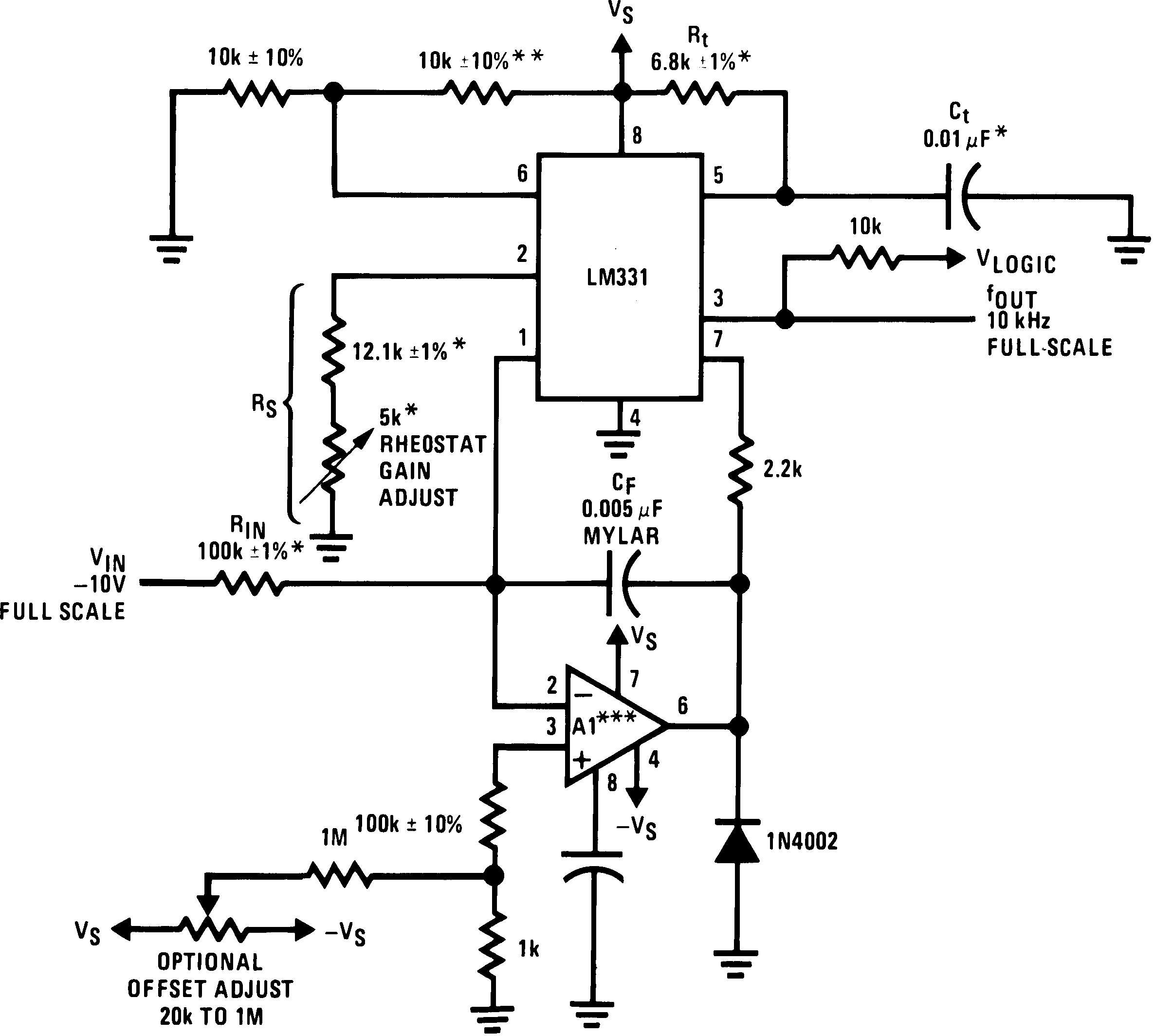

**This resistor can be 5 kΩ or 10 kΩ for VS = 8 V to 22 V, but must be 10 kΩ for VS = 4.5 V to 8 V.
***Use low offset voltage and low offset current op-amps for A1: recommended type LF411A
9.3 System Examples
9.3.1 F-to-V Converters
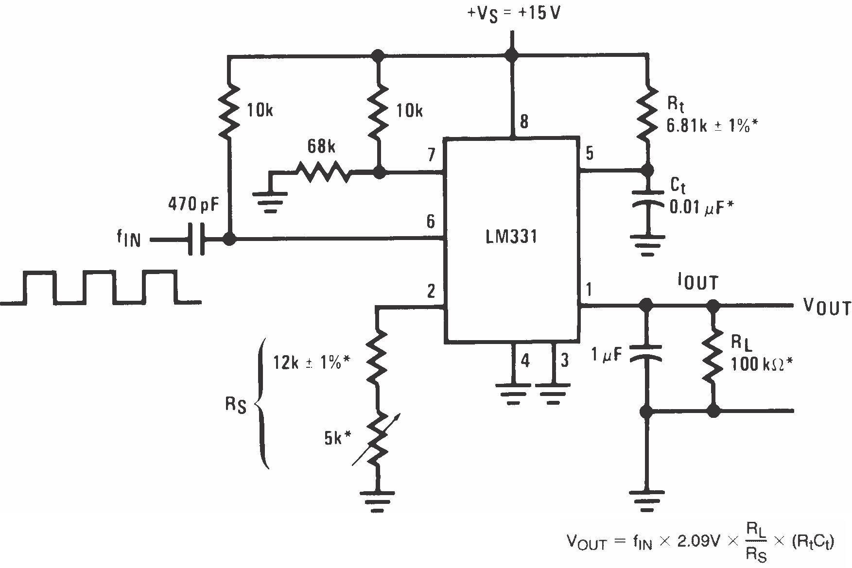
In these applications, a pulse input at fIN is differentiated by a C-R network and the negative-going edge at pin 6 causes the input comparator to trigger the timer circuit. Just as with a V-to-F converter, the average current flowing out of pin 1 is IAVERAGE = i × (1.1 RtCt) × f.
In the simple circuit of Figure 18, this current is filtered in the network RL = 100 kΩ and 1 μF. The ripple will be less than 10-mV peak, but the response will be slow, with a 0.1 second time constant, and settling of 0.7 second to 0.1% accuracy.
In the precision circuit, an operational amplifier provides a buffered output and also acts as a 2-pole filter. The ripple will be less than 5-mV peak for all frequencies above 1 kHz, and the response time will be much quicker than in Figure 18. However, for input frequencies below 200 Hz, this circuit will have worse ripple than Figure 18. The engineering of the filter time-constants to get adequate response and small enough ripple simply requires a study of the compromises to be made. Inherently, V-to-F converter response can be fast, but F-to-V response can not.
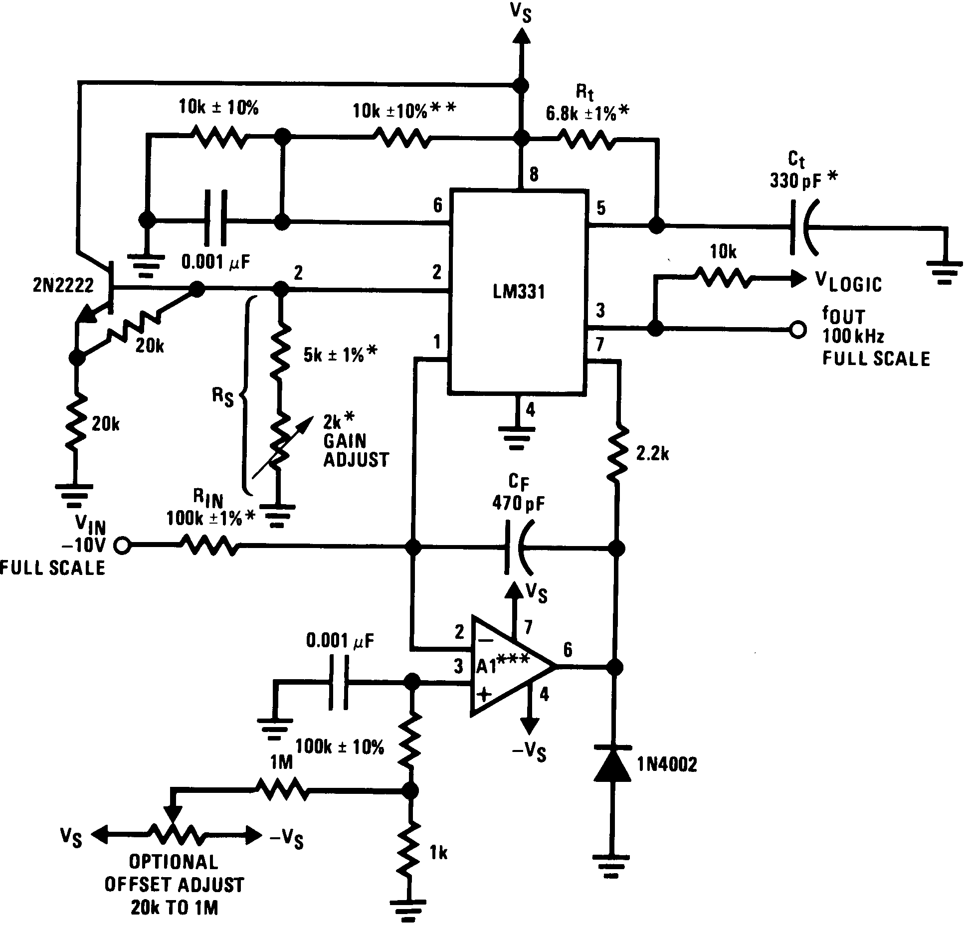
*Use stable components with low temperature coefficients.
**This resistor can be 5 kΩ or 10 kΩ for VS=8V to 22V, but must be 10 kΩ for VS=4.5V to 8V.
***Use low offset voltage and low offset current op-amps for A1: recommended types LF411A or LF356.
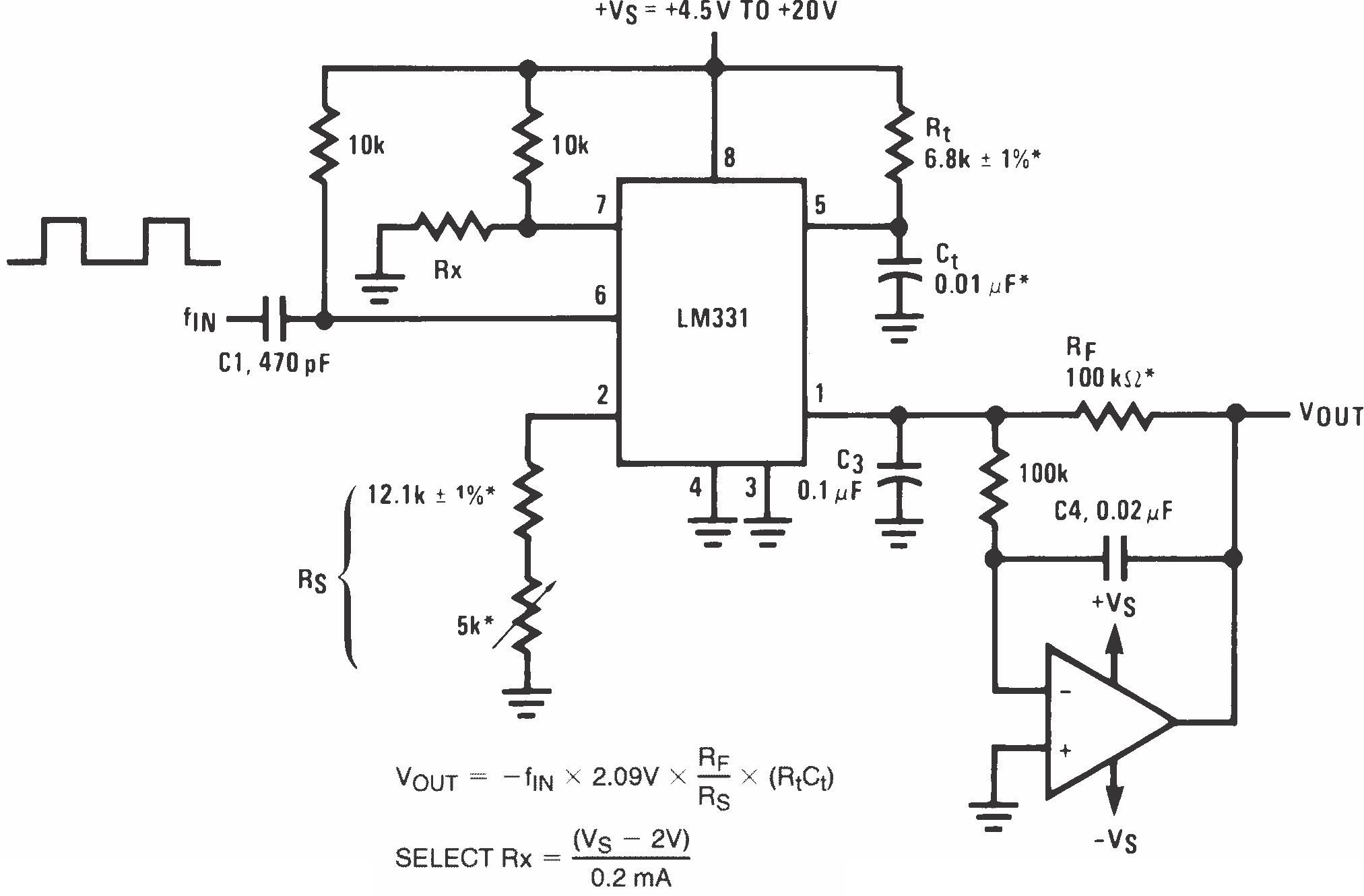
*Use stable components with low temperature coefficients.
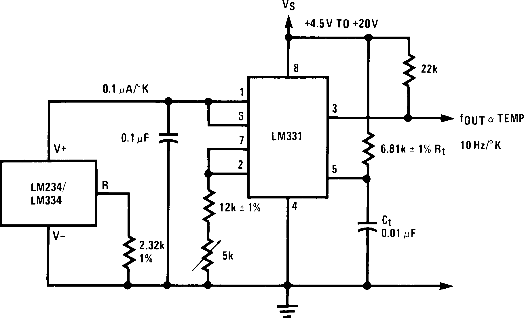 Figure 21. Temperature to Frequency Converter
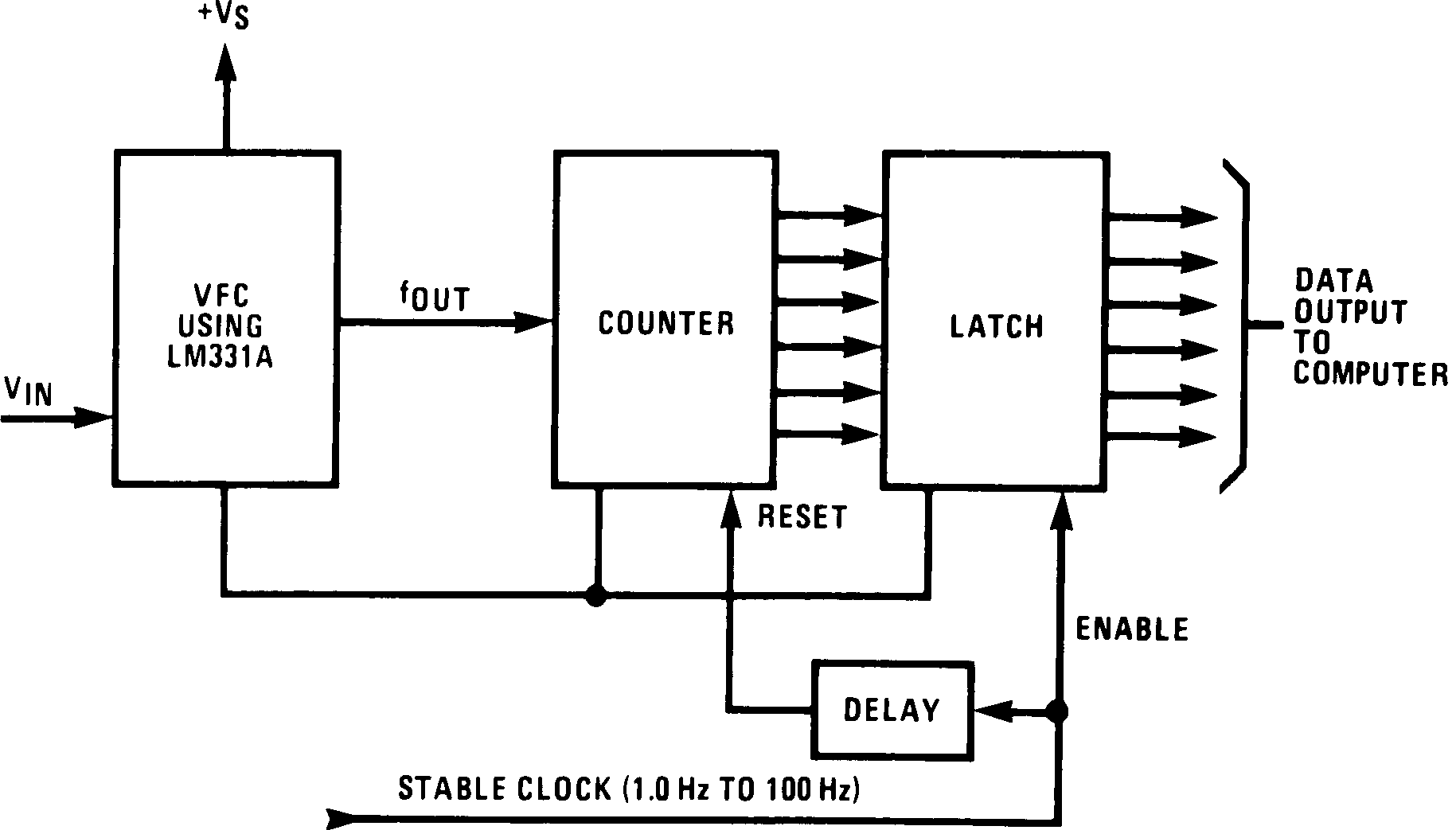 Figure 23. Basic Analog-to-Digital Converter Using
Voltage-to-Frequency Converter
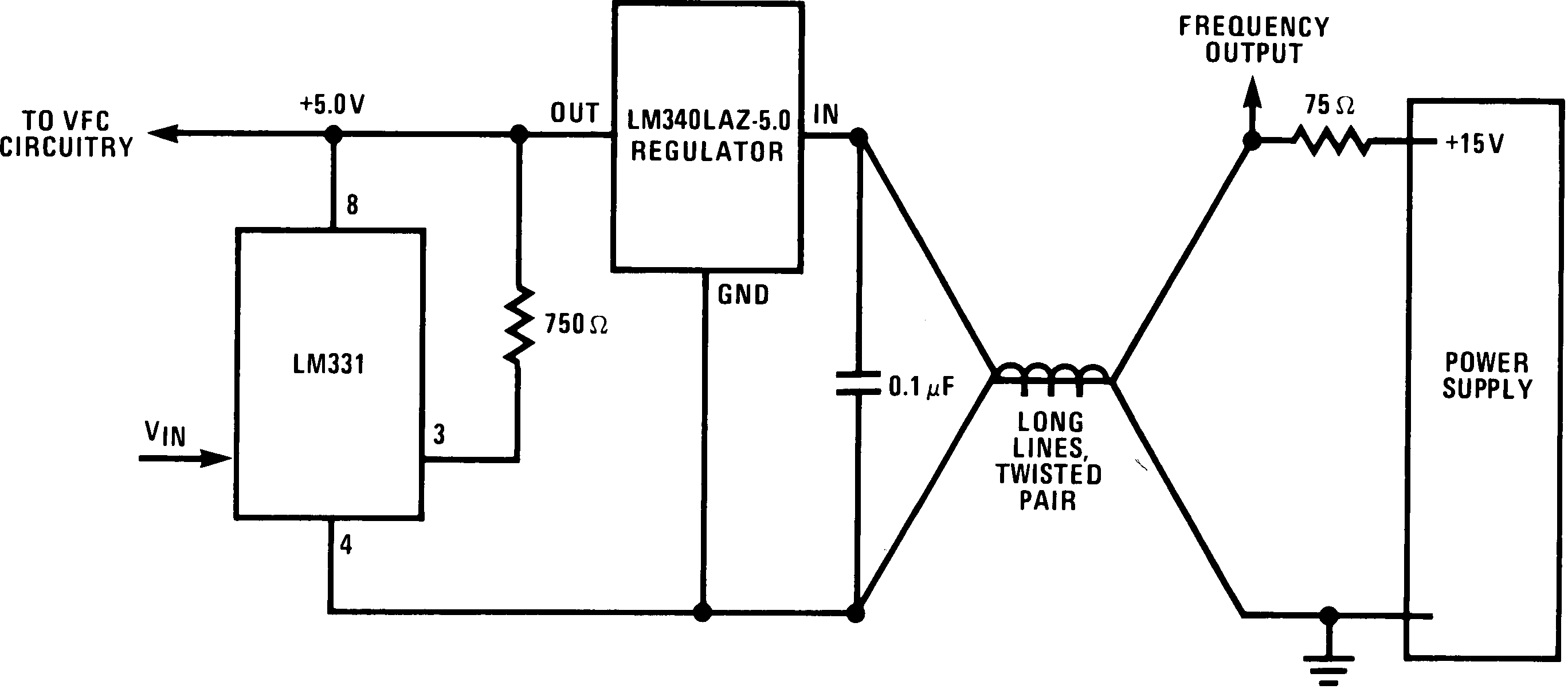 Figure 25. Remote Voltage-to-Frequency Converter With 2-Wire Transmitter and Receiver
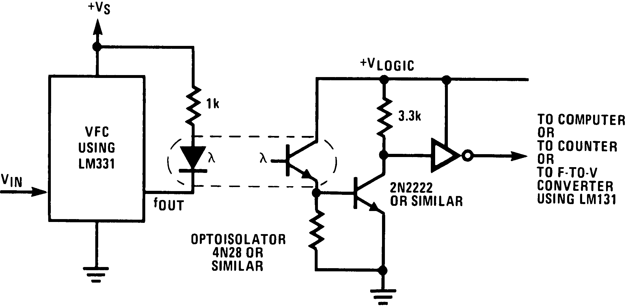 Figure 27. Voltage-to-Frequency Converter With Isolators
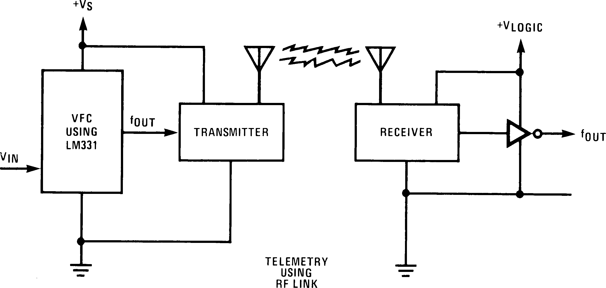 Figure 29. Voltage-to-Frequency Converter With Isolators
*Use stable components with low temperature coefficients.
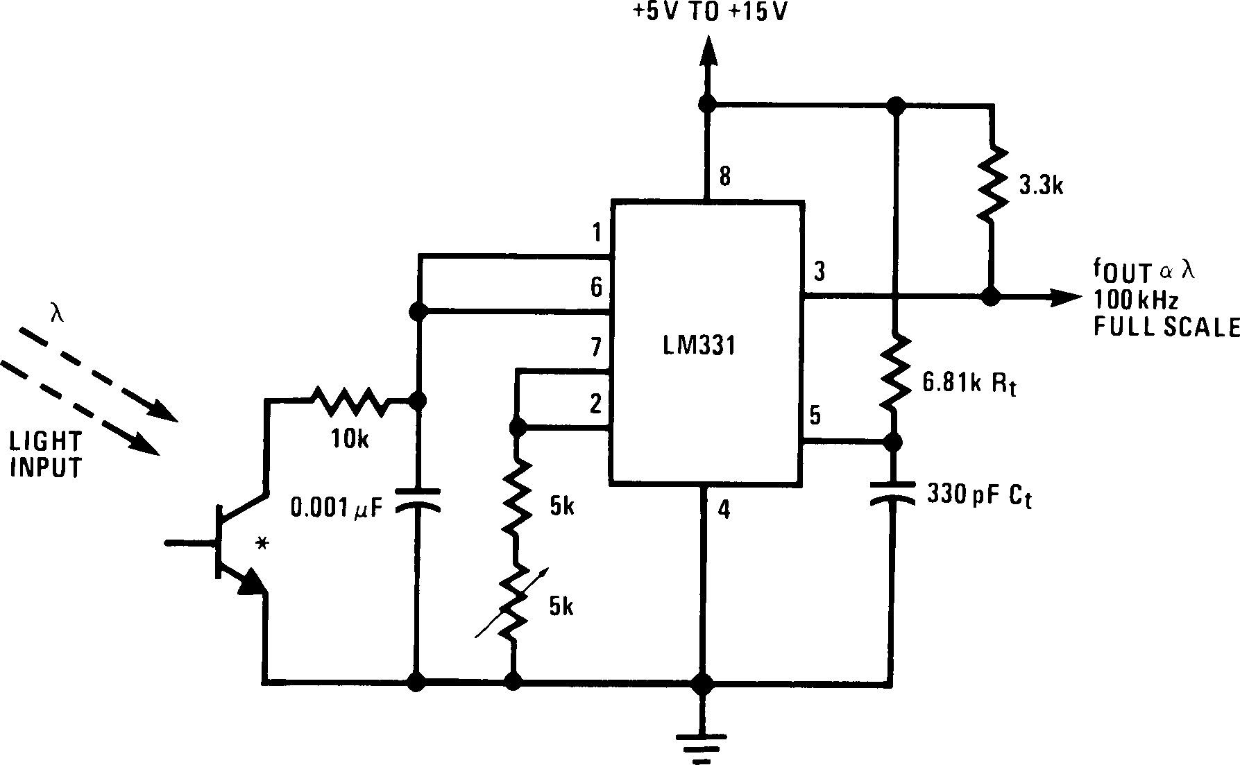
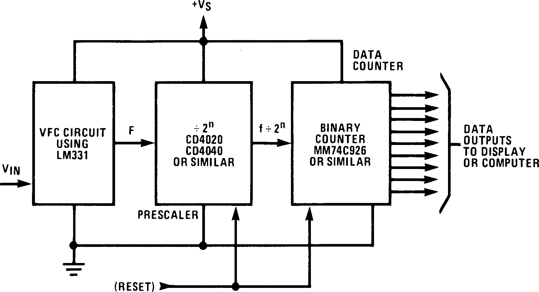 Figure 22. Long-Term Digital Integrator Using VFC
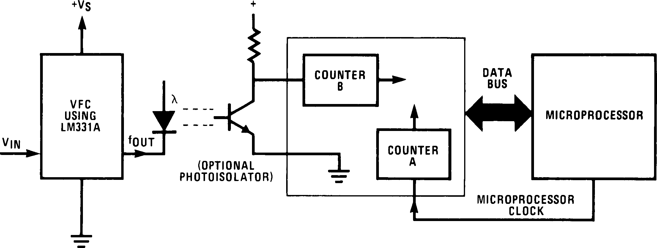 Figure 24. Analog-to-Digital Converter With Microprocessor
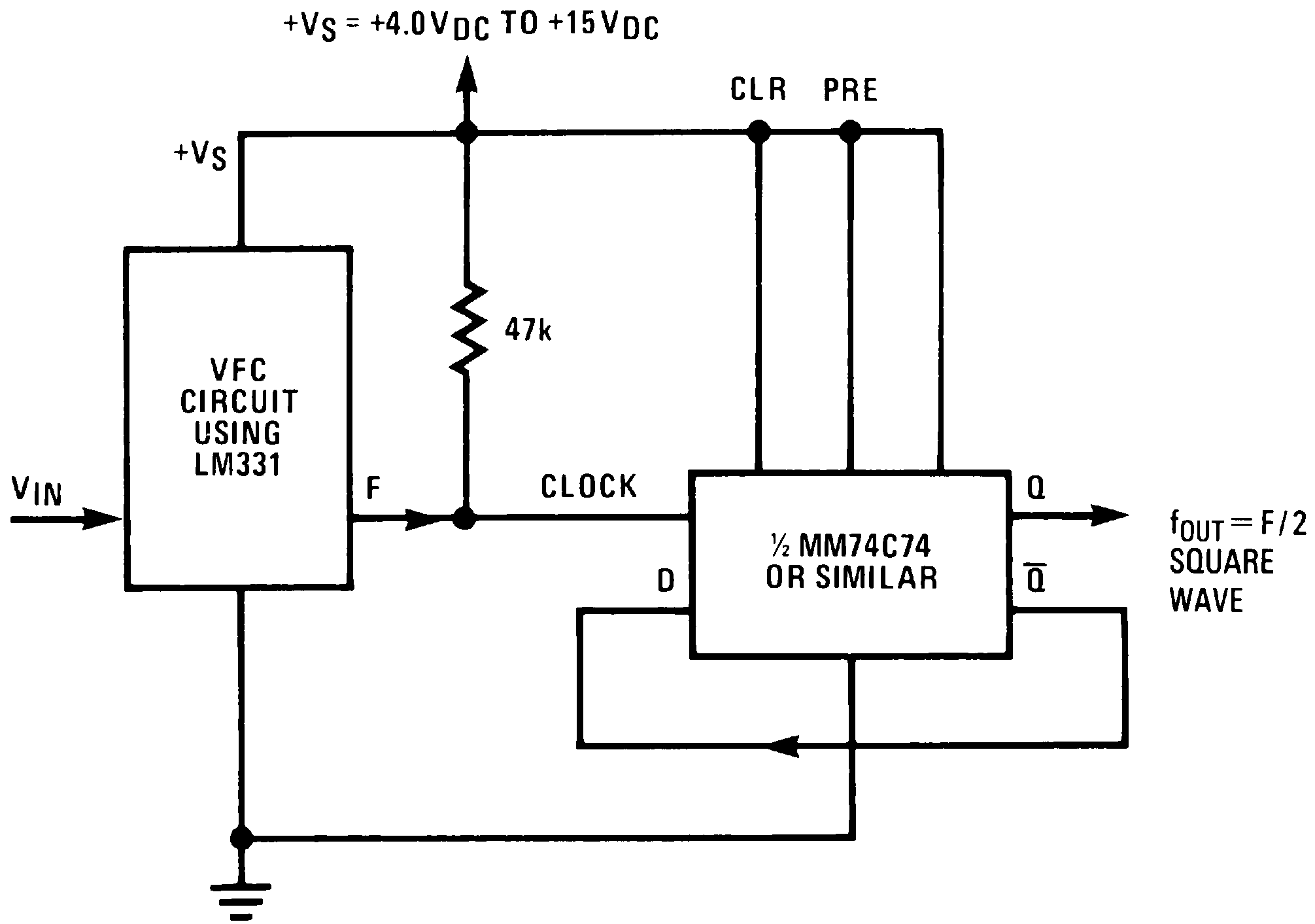 Figure 26. Voltage-to-Frequency Converter With Square-Wave Output Using ÷ 2 Flip-Flop
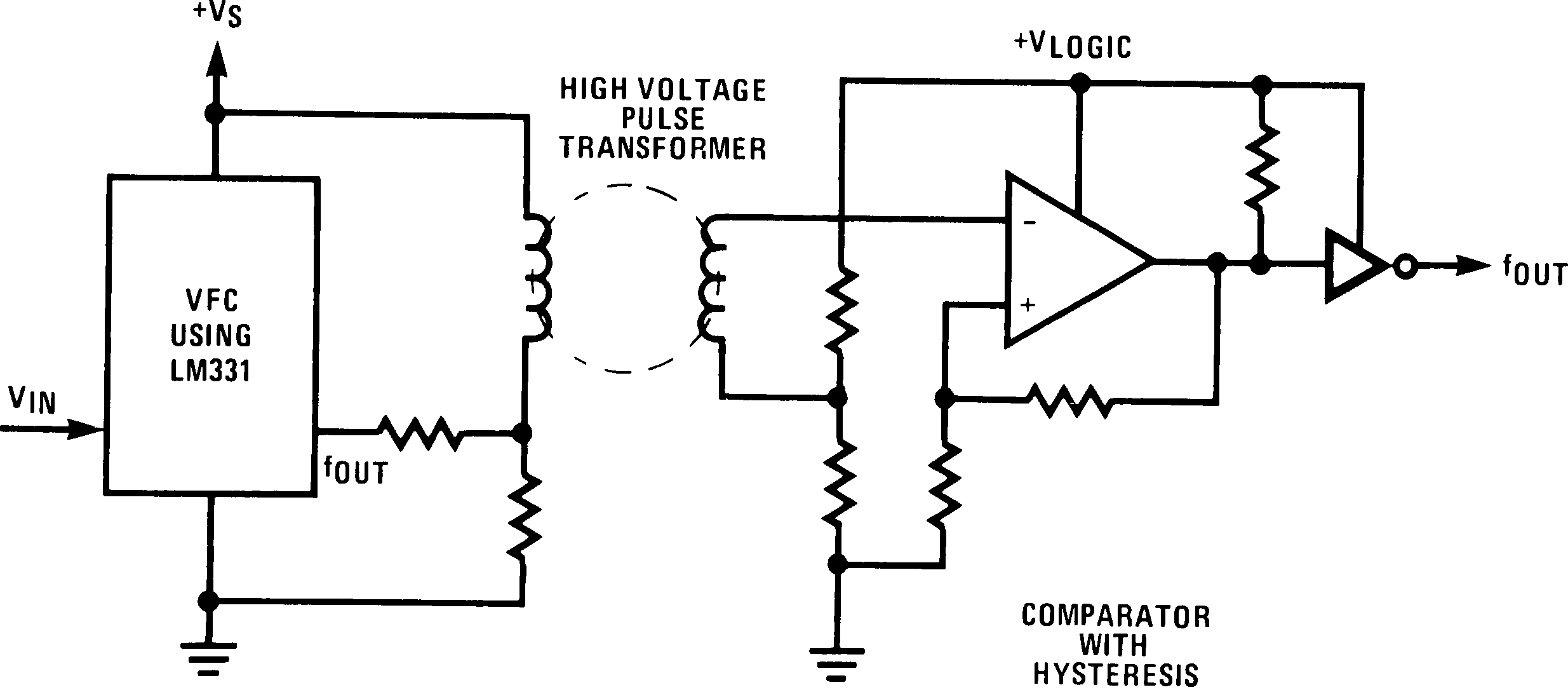 Figure 28. Voltage-to-Frequency Converter With Isolators
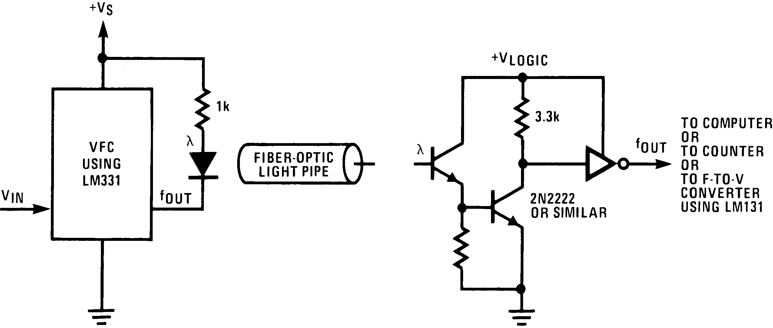 Figure 30. Voltage-to-Frequency Converter With Isolators