SNVSAX3 June   2017 LM337-N-MIL

PRODUCTION DATA.  

  1. Features
  2. Applications
  3. Description
  4. Revision History
  5. Pin Configuration and Functions
  6. Specifications
    1. 6.1 Absolute Maximum Ratings
    2. 6.2 ESD Ratings
    3. 6.3 Recommended Operating Conditions
    4. 6.4 Thermal Information
    5. 6.5 Electrical Characteristics
    6. 6.6 Typical Characteristics
  7. Detailed Description
    1. 7.1 Overview
    2. 7.2 Functional Block Diagram
    3. 7.3 Feature Description
      1. 7.3.1 Thermal Regulation
    4. 7.4 Device Functional Modes
      1. 7.4.1 Protection Diodes
  8. Application and Implementation
    1. 8.1 Application Information
    2. 8.2 Typical Applications
      1. 8.2.1 Adjustable Negative Voltage Regulator
        1. 8.2.1.1 Design Requirements
        2. 8.2.1.2 Detailed Design Procedure
        3. 8.2.1.3 Application Curve
      2. 8.2.2 Adjustable Lab Voltage Regulator
      3. 8.2.3 −5.2-V Regulator with Electronic Shutdown
      4. 8.2.4 High Stability −10-V Regulator
  9. Power Supply Recommendations
  10. 10Layout
    1. 10.1 Layout Guidelines
    2. 10.2 Layout Example
    3. 10.3 Thermal Considerations
      1. 10.3.1 Heatsinking SOT-223 Package Parts
  11. 11Device and Documentation Support
    1. 11.1 Documentation Support
      1. 11.1.1 Related Documentation
    2. 11.2 Community Resources
    3. 11.3 Trademarks
    4. 11.4 Electrostatic Discharge Caution
    5. 11.5 Glossary
  12. 12Mechanical, Packaging, and Orderable Information

Package Options

Mechanical Data (Package|Pins)
Thermal pad, mechanical data (Package|Pins)
Orderable Information

Pin Configuration and Functions

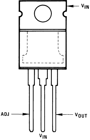
TO-220 Plastic Package
Package Number NDE0003B
Front View
LM337-N-MIL 00906707.png
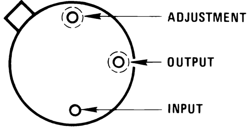
TO Metal Can Package
3-Pin Package Number NDT0003A
Bottom View
LM337-N-MIL 00906706.png
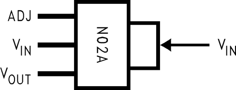
SOT-223
3-Lead Package Marked N02A
Front View
LM337-N-MIL 00906734.png

Pin Functions

PIN I/O DESCRIPTION
NAME TO-220 TO SOT-223
ADJ 1 1 1 Adjust pin
VIN 2, TAB 3, CASE 2, 4 I Input voltage pin for the regulator
VOUT 3 2 3 O Output voltage pin for the regulator