SNOSBT0L February   2000  – September 2016 LM340

PRODUCTION DATA.  

  1. Features
  2. Applications
    1.     Available Packages
  3. Description
    1.     Fixed Output Voltage Regulator
  4. Revision History
  5. Pin Configuration and Functions
    1.     Pin Functions
  6. Specifications
    1. 6.1 Absolute Maximum Ratings
    2. 6.2 ESD Ratings
    3. 6.3 Recommended Operating Conditions
    4. 6.4 Thermal Information
    5. 6.5 LM340A Electrical Characteristics, VO = 5 V, VI = 10 V
    6. 6.6 LM340 / LM7805 Electrical Characteristics, VO = 5 V, VI = 10 V
    7. 6.7 LM340 / LM7812 Electrical Characteristics, VO = 12 V, VI = 19 V
    8. 6.8 LM340 / LM7815 Electrical Characteristics, VO = 15 V, VI = 23 V
    9. 6.9 Typical Characteristics
  7. Detailed Description
    1. 7.1 Overview
    2. 7.2 Functional Block Diagram
    3. 7.3 Feature Description
      1. 7.3.1 Output Current
      2. 7.3.2 Current Limiting Feature
      3. 7.3.3 Thermal Shutdown
    4. 7.4 Device Functional Modes
  8. Application and Implementation
    1. 8.1 Application Information
      1. 8.1.1 Shorting the Regulator Input
      2. 8.1.2 Raising the Output Voltage Above the Input Voltage
      3. 8.1.3 Regulator Floating Ground
      4. 8.1.4 Transient Voltages
    2. 8.2 Typical Applications
      1. 8.2.1 Fixed Output Voltage Regulator
        1. 8.2.1.1 Design Requirements
        2. 8.2.1.2 Detailed Design Procedure
        3. 8.2.1.3 Application Curve
    3. 8.3 System Examples
  9. Power Supply Recommendations
  10. 10Layout
    1. 10.1 Layout Guidelines
    2. 10.2 Layout Example
    3. 10.3 Heat Sinking DDPAK/TO-263 and SOT-223 Package Parts
  11. 11Device and Documentation Support
    1. 11.1 Documentation Support
      1. 11.1.1 Related Documentation
    2. 11.2 Related Links
    3. 11.3 Receiving Notification of Documentation Updates
    4. 11.4 Community Resources
    5. 11.5 Trademarks
    6. 11.6 Electrostatic Discharge Caution
    7. 11.7 Glossary
  12. 12Mechanical, Packaging, and Orderable Information

Package Options

Mechanical Data (Package|Pins)
Thermal pad, mechanical data (Package|Pins)
Orderable Information

Typical Characteristics

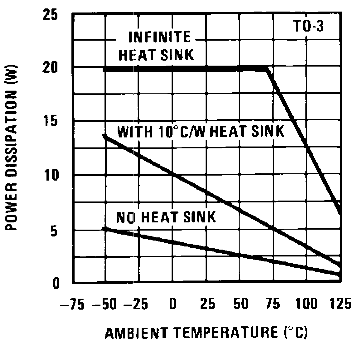
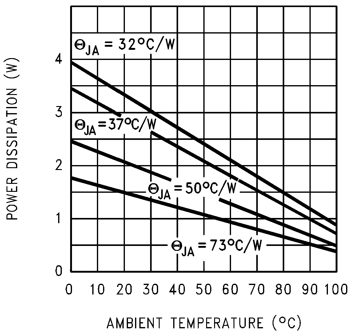
LM340 LM340A LM7805 LM7812 LM7815 00778122.pngFigure 1. Maximum Average Power Dissipation
LM340 LM340A LM7805 LM7812 LM7815 00778124.png
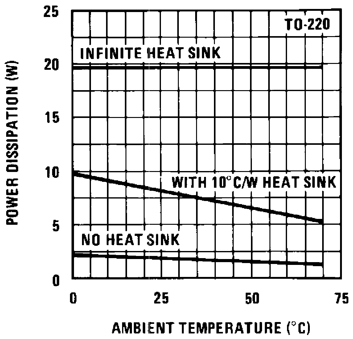
Figure 3. Maximum Power Dissipation (DDPAK/TO-263)
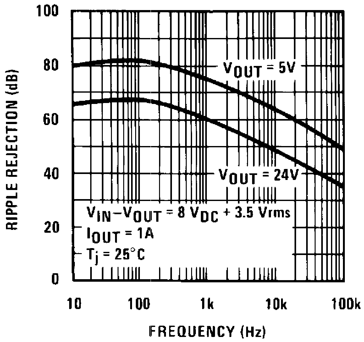
LM340 LM340A LM7805 LM7812 LM7815 00778126.pngFigure 5. Ripple Rejection
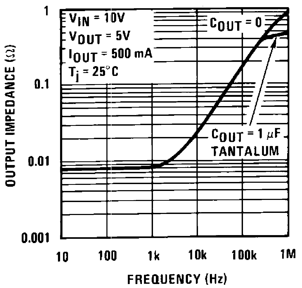
LM340 LM340A LM7805 LM7812 LM7815 00778128.pngFigure 7. Output Impedance
LM340 LM340A LM7805 LM7812 LM7815 00778130.png
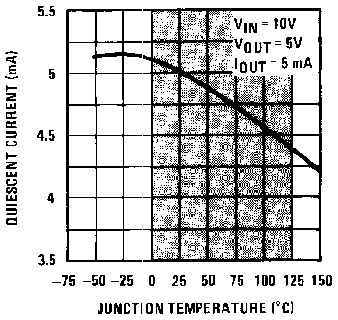
Shaded area refers to LM340A/LM340, LM7805, LM7812, and LM7815.
Figure 9. Quiescent Current
LM340 LM340A LM7805 LM7812 LM7815 00778132.png
Shaded area refers to LM340A/LM340, LM7805, LM7812, and LM7815.
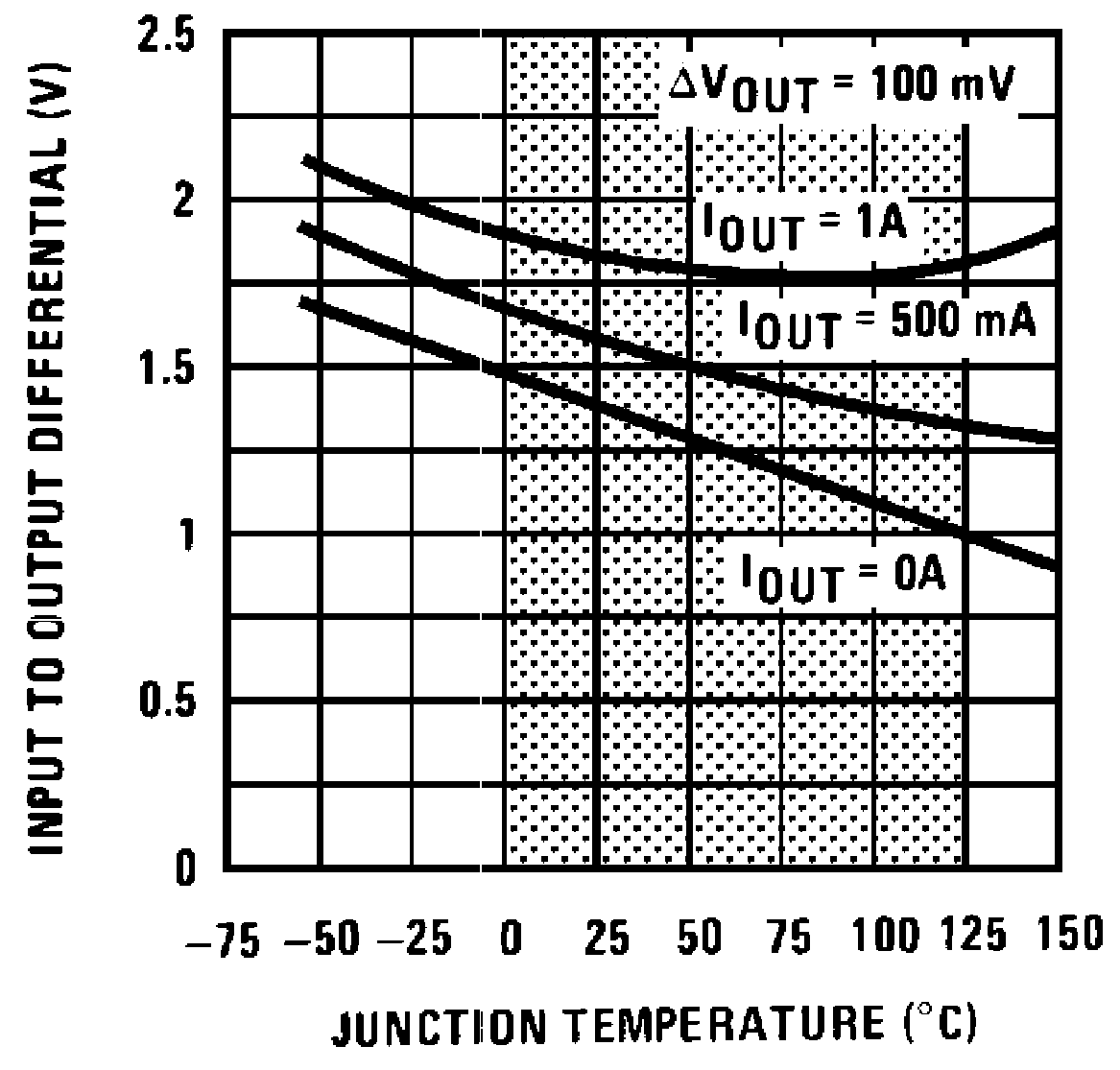
Figure 11. Dropout Voltage
LM340 LM340A LM7805 LM7812 LM7815 00778105.png
IOUT = 1 A, TA = 25°C
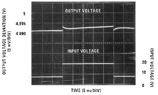
Figure 13. Line Regulation LM340
LM340 LM340A LM7805 LM7812 LM7815 00778123.pngFigure 2. Maximum Average Power Dissipation
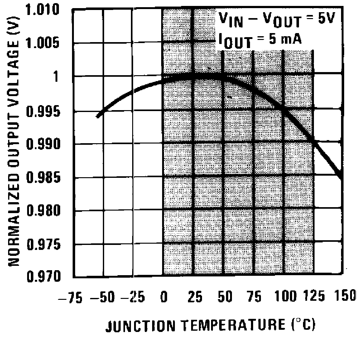
LM340 LM340A LM7805 LM7812 LM7815 00778125.png
Shaded area refers to LM340A/LM340, LM7805, LM7812 and LM7815.
Figure 4. Output Voltage (Normalized to 1 V at TJ = 25°C)
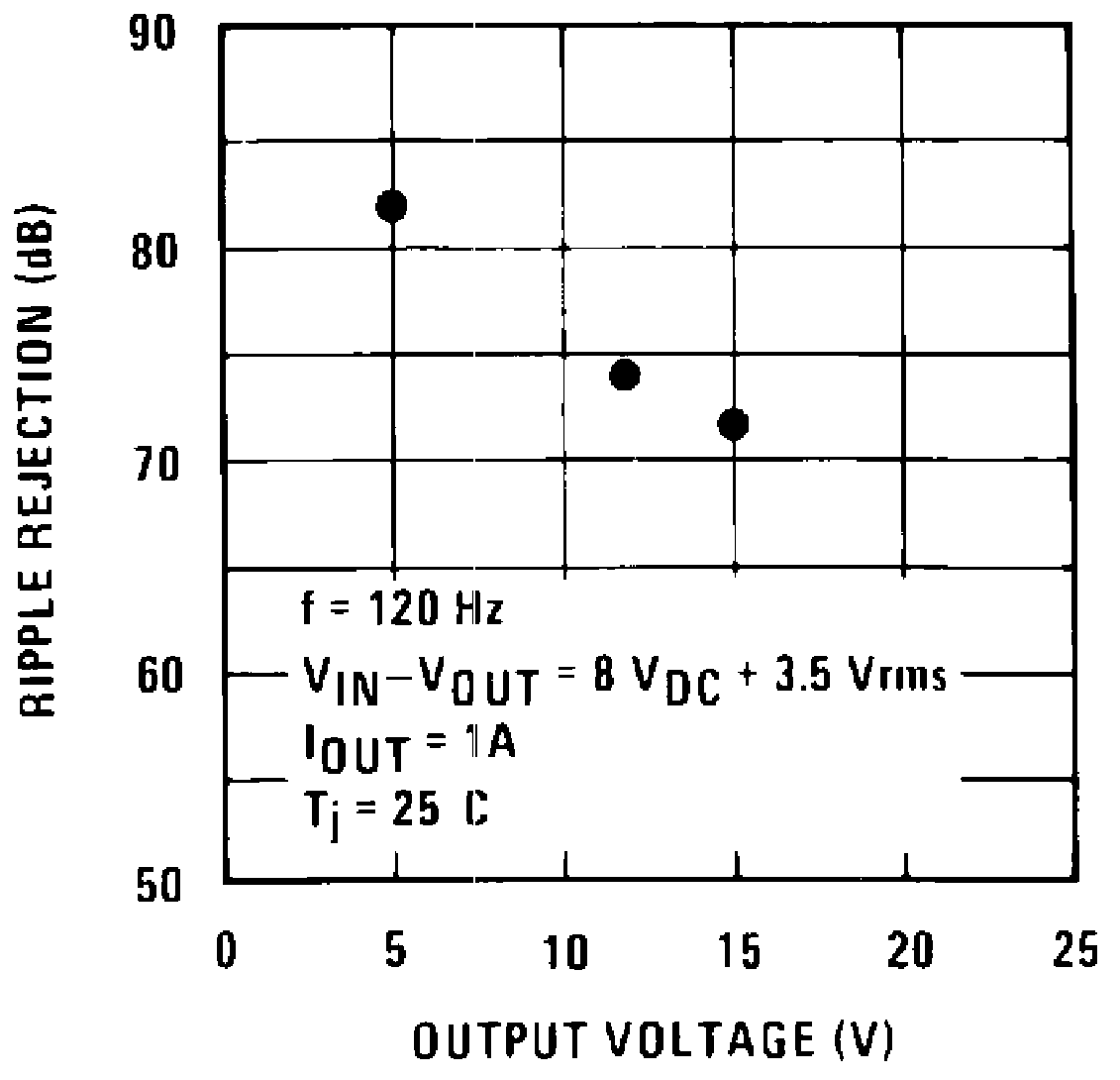
LM340 LM340A LM7805 LM7812 LM7815 00778127.pngFigure 6. Ripple Rejection
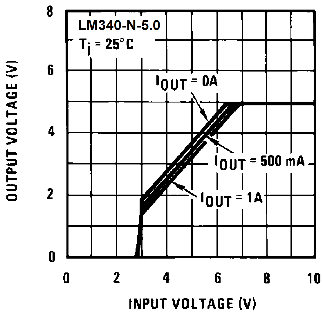
LM340 LM340A LM7805 LM7812 LM7815 00778129_1.pngFigure 8. Dropout Characteristics
LM340 LM340A LM7805 LM7812 LM7815 00778131.png
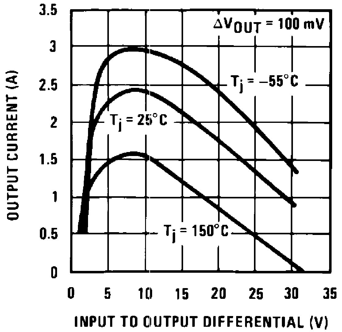
Figure 10. Peak Output Current
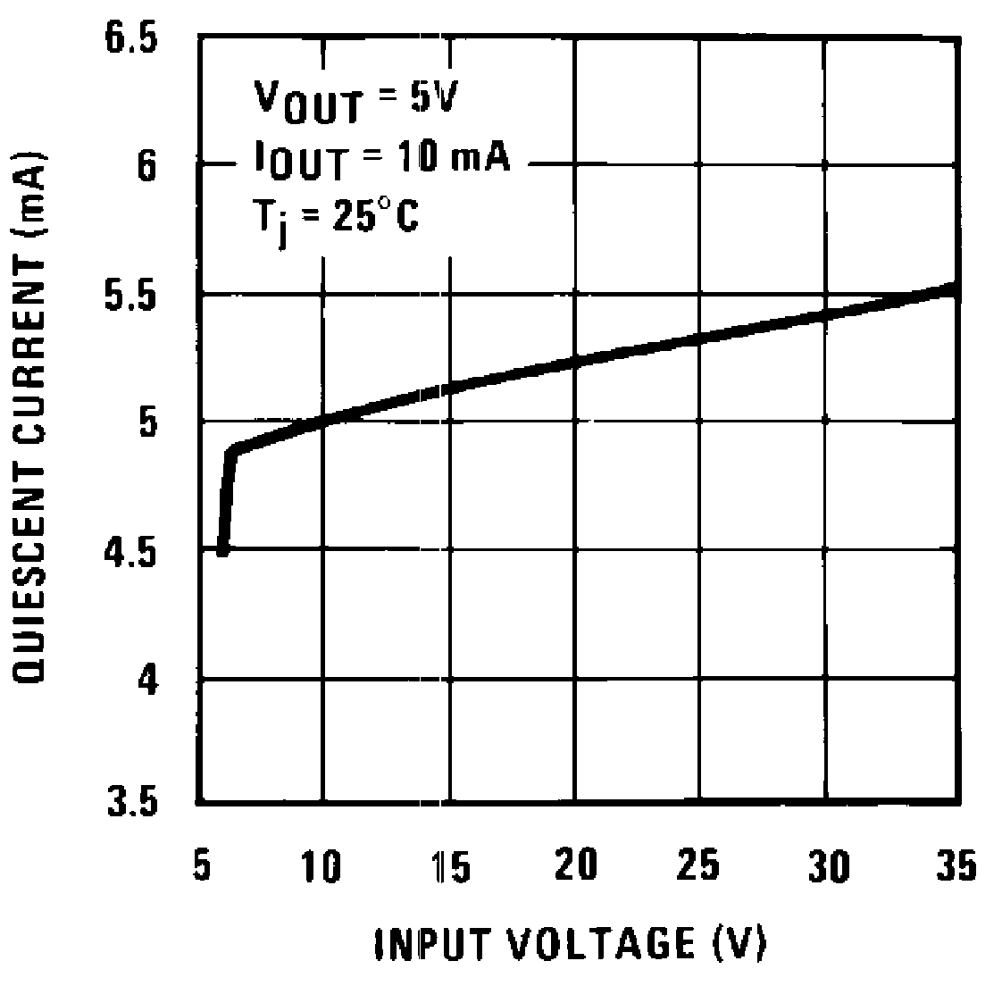
LM340 LM340A LM7805 LM7812 LM7815 00778133.pngFigure 12. Quiescent Current
LM340 LM340A LM7805 LM7812 LM7815 00778106.png
VIN = 10 V, TA = 25°C
Figure 14. Line Regulation LM340