SNVS541H October 2007 – August 2016 LM3410 , LM3410-Q1
PRODUCTION DATA.
- 1 Features
- 2 Applications
- 3 Description
- 4 Revision History
- 5 Pin Configuration and Functions
- 6 Specifications
- 7 Detailed Description
-
8 Application and Implementation
- 8.1 Application Information
- 8.2
Typical Applications
- 8.2.1 Low Input Voltage, 1.6-MHz, 3 to 5 White LED Output at 50-mA Boost Converter
- 8.2.2 LM3410X SOT-23: 5 × 1206 Series LED String Application
- 8.2.3 LM3410Y SOT-23: 5 × 1206 Series LED String Application
- 8.2.4 LM3410X WSON: 7 × 5 LED Strings Backlighting Application
- 8.2.5 LM3410X WSON: 3 × HB LED String Application
- 8.2.6 LM3410Y SOT-23: 5 × 1206 Series LED String Application With OVP
- 8.2.7 LM3410X SEPIC WSON: HB or OLED Illumination Application
- 8.2.8 LM3410X WSON: Boost Flash Application
- 8.2.9 LM3410X SOT-23: 5 × 1206 Series LED String Application With VIN > 5.5 V
- 8.2.10 LM3410X WSON: Camera Flash or Strobe Circuit Application
- 8.2.11 LM3410X SOT-23: 5 × 1206 Series LED String Application With VIN and VPWR Rail > 5.5 V
- 8.2.12 LM3410X WSON: Boot-Strap Circuit to Extend Battery Life
- 9 Power Supply Recommendations
- 10Layout
- 11Device and Documentation Support
- 12Mechanical, Packaging, and Orderable Information
Package Options
Mechanical Data (Package|Pins)
Thermal pad, mechanical data (Package|Pins)
- DGN|8
Orderable Information
7 Detailed Description
7.1 Overview
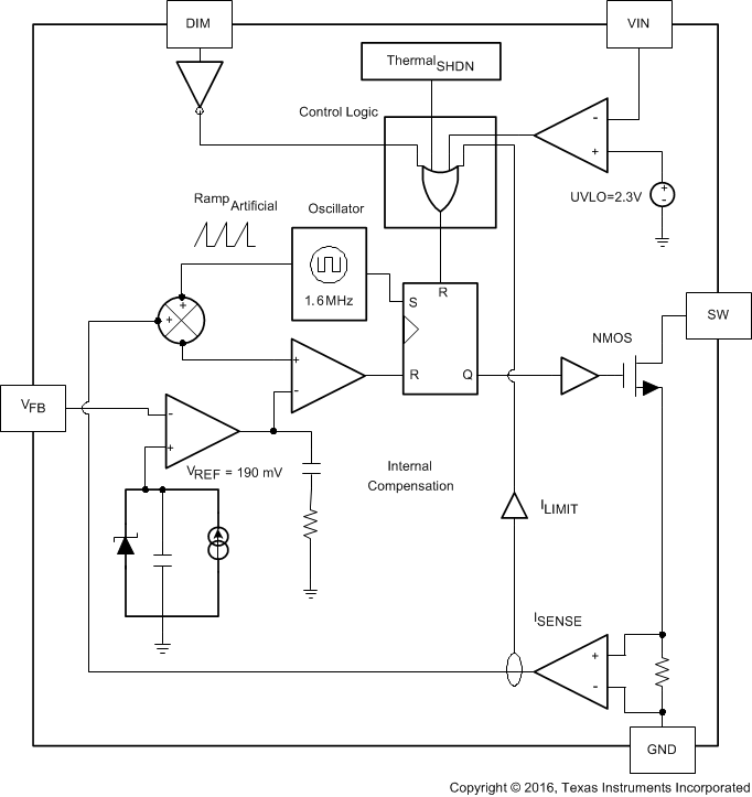
The LM3410 and LM3410-Q1 are a constant frequency PWM, boost regulator IC. It delivers a minimum of 2.1-A peak switch current. The device operates very similar to a voltage regulated boost converter except that the device regulates the output current that passes through LEDs. The current magnitude is set with a series resistor. The converter regulates to the feedback voltage (190 mV) created by the multiplication of the series resistor and the LED current. The regulator has a preset switching frequency of either 525 kHz or 1.6 MHz. This high frequency allows the LM3410 or LM3410-Q1 to operate with small surface mount capacitors and inductors, resulting in a DC-DC converter that requires a minimum amount of board space. The LM3410 and LM3410-Q1 are internally compensated and requires few external components, making usage simple. The LM3410 and LM3410-Q1 use current-mode control to regulate the LED current.
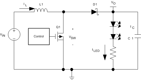
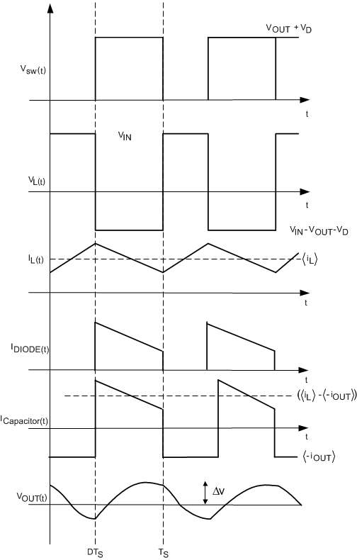
The LM3410 and LM3410-Q1 supply a regulated LED current by switching the internal NMOS control switch at constant frequency and variable duty cycle. A switching cycle begins at the falling edge of the reset pulse generated by the internal oscillator. When this pulse goes low, the output control logic turns on the internal NMOS control switch. During this ON time, the SW pin voltage (VSW) decreases to approximately GND, and the inductor current (IL) increases with a linear slope. IL is measured by the current sense amplifier, which generates an output proportional to the switch current. The sensed signal is summed with the regulator’s corrective ramp and compared to the error amplifier’s output, which is proportional to the difference between the feedback voltage and reference voltage (VREF). When the PWM comparator output goes high, the output switch turns off until the next switching cycle begins. During the switch OFF time, inductor current discharges through diode D1, which forces the SW pin to swing to the output voltage plus the forward voltage (VD) of the diode. The regulator loop adjusts the duty cycle (D) to maintain a regulated LED current.
 Figure 10. Simplified Boost Topology Schematic
 Figure 11. Typical Waveforms
7.2 Functional Block Diagram

7.3 Feature Description
7.3.1 Current Limit
The LM3410 and LM3410-Q1 use cycle-by-cycle current limiting to protect the internal NMOS switch. This current limit does not protect the output from excessive current during an output short circuit. The input supply is connected to the output by the series connection of an inductor and a diode. If a short circuit is placed on the output, excessive current can damage both the inductor and diode.
7.3.2 DIM Pin and Shutdown Mode
The average LED current can be controlled using a PWM signal on the DIM pin. The duty cycle can be varied from 0 to 100%, to either increase or decrease LED brightness. PWM frequencies from 1 Hz to 25 kHz can be used. For controlling LED currents down to the µA levels, it is best to use a PWM signal frequency from 200 to 1 kHz. The maximum LED current would be achieved using a 100% duty cycle, that is the DIM pin always high.
7.4 Device Functional Modes
7.4.1 Thermal Shutdown
Thermal shutdown limits total power dissipation by turning off the output switch when the IC junction temperature exceeds 165°C. After thermal shutdown occurs, the output switch does not turn on until the junction temperature drops to approximately 150°C.