SNVS239C October 2004 – October 2015 LM3475
PRODUCTION DATA.
- 1 Features
- 2 Applications
- 3 Description
- 4 Revision History
- 5 Pin Configuration and Functions
- 6 Specifications
- 7 Detailed Description
-
8 Application and Implementation
- 8.1 Application Information
- 8.2
Typical Application
- 8.2.1 Design Requirements
- 8.2.2
Detailed Design Procedure
- 8.2.2.1 Setting Output Voltage
- 8.2.2.2 Setting Operating Frequency and Output Ripple
- 8.2.2.3 Using a Feed-forward Capacitor
- 8.2.2.4 Inductor Selection
- 8.2.2.5 Output Capacitor Selection
- 8.2.2.6 Input Capacitor Selection
- 8.2.2.7 Diode Selection
- 8.2.2.8 P-Channel MOSFET Selection
- 8.2.2.9 Reducing Switching Noise
- 8.2.3 Application Curves
- 9 Power Supply Recommendations
- 10Layout
- 11Device and Documentation Support
- 12Mechanical, Packaging, and Orderable Information
Package Options
Mechanical Data (Package|Pins)
- DBV|5
Thermal pad, mechanical data (Package|Pins)
Orderable Information
10 Layout
10.1 Layout Guidelines
PC board layout is very important in all switching regulator designs. Poor layout can cause EMI problems, excess switching noise and poor operation.
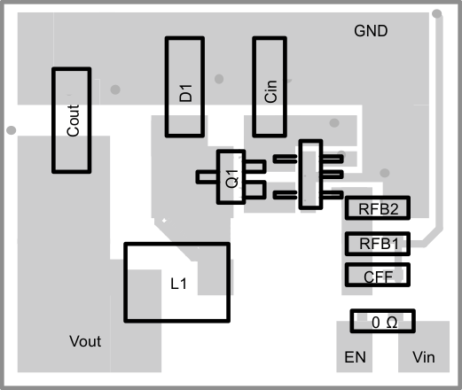
As shown in Figure 16, place the ground of the input capacitor as close as possible to the anode of the diode. This path also carries a large AC current. The switch node, the node connecting the diode cathode, inductor, and PFET drain, should be kept as small as possible. This node is one of the main sources for radiated EMI.
The feedback pin is a high impedance node and is therefore sensitive to noise. Be sure to keep all feedback traces away from the inductor and the switch node, which are sources of noise. Also, the resistor divider should be placed close to the FB pin. The gate pin of the external PFET should be located close to the PGATE pin.
TI also recommends using a large, continuous ground plane, particularly in higher current applications.
10.2 Layout Example
 Figure 16. Layout Example (2:1 Scale)