SNVS346H November 2007 – October 2024 LM3481
PRODUCTION DATA
- 1
- 1 Features
- 2 Applications
- 3 Description
- 4 Pin Configuration and Functions
- 5 Specifications
- 6 Detailed Description
-
7 Application and Implementation
- 7.1 Application Information
- 7.2
Typical Applications
- 7.2.1
Boost Converter
- 7.2.1.1 Design Requirements
- 7.2.1.2
Detailed Design Procedure
- 7.2.1.2.1 Custom Design with WEBENCH Tools
- 7.2.1.2.2 Power Inductor Selection
- 7.2.1.2.3 Programming the Output Voltage and Output Current
- 7.2.1.2.4 Current Limit With Additional Slope Compensation
- 7.2.1.2.5 Power Diode Selection
- 7.2.1.2.6 Power MOSFET Selection
- 7.2.1.2.7 Input Capacitor Selection
- 7.2.1.2.8 Output Capacitor Selection
- 7.2.1.2.9 Driver Supply Capacitor Selection
- 7.2.1.2.10 Compensation
- 7.2.1.3 Application Curve
- 7.2.2 Typical SEPIC Converter
- 7.2.1
Boost Converter
- 7.3 Power Supply Recommendations
- 7.4 Layout
- 8 Device and Documentation Support
- 9 Revision History
- 10Mechanical, Packaging, and Orderable Information
Package Options
Mechanical Data (Package|Pins)
- DGS|10
Thermal pad, mechanical data (Package|Pins)
Orderable Information
7.2.2.2.1 Power MOSFET Selection
As in a boost converter, the parameters governing the selection of the MOSFET are the minimum threshold voltage, VTH(MIN), the on-resistance, RDS(ON), the total gate charge, Qg, the reverse transfer capacitance, CRSS, and the maximum drain to source voltage, VDS(MAX). The peak switch voltage in a SEPIC is given by:
Equation 44. VSW(PEAK) = VIN + VOUT + VDIODE
The selected MOSFET should satisfy the condition:
Equation 45. VDS(MAX) > VSW(PEAK)
The peak switch current is given by:
Equation 46. 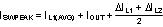
Where ΔIL1 and ΔIL2 are the peak-to-peak inductor ripple currents of inductors L1 and L2 respectively.
The rms current through the switch is given by:
Equation 47. 