SNVS178H January 2002 – December 2015 LM3485
PRODUCTION DATA.
- 1 Features
- 2 Applications
- 3 Description
- 4 Revision History
- 5 Pin Configuration and Functions
- 6 Specifications
- 7 Detailed Description
-
8 Application and Implementation
- 8.1 Application Information
- 8.2
Typical Application
- 8.2.1 Design Requirements
- 8.2.2
Detailed Design Procedure
- 8.2.2.1 Step by Step Design Procedure
- 8.2.2.2 Inductor Selection (L1)
- 8.2.2.3 Output Voltage Set Point
- 8.2.2.4 Output Capacitor Selection (COUT)
- 8.2.2.5 Input Capacitor Selection (CIN)
- 8.2.2.6 Programming the Current Limit (RADJ)
- 8.2.2.7 Catch Diode Selection (D1)
- 8.2.2.8 P-Channel MOSFET Selection (Q1)
- 8.2.3 Application Curves
- 9 Power Supply Recommendations
- 10Layout
- 11Device and Documentation Support
- 12Mechanical, Packaging, and Orderable Information
Package Options
Mechanical Data (Package|Pins)
- DGK|8
Thermal pad, mechanical data (Package|Pins)
Orderable Information
8 Application and Implementation
NOTE
Information in the following applications sections is not part of the TI component specification, and TI does not warrant its accuracy or completeness. TI’s customers are responsible for determining suitability of components for their purposes. Customers should validate and test their design implementation to confirm system functionality.
8.1 Application Information
Hysteretic control is a simple control scheme. However the operating frequency and other performance characteristics highly depend on external conditions and components. If either the inductance, output capacitance, ESR, VIN, or Cff is changed, there will be a change in the operating frequency and output ripple. The best approach is to determine what operating frequency is desirable in the application and then begin with the selection of the inductor and COUT ESR.
8.2 Typical Application
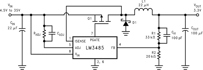
 Figure 27. Typical Application Schematic
8.2.1 Design Requirements
For this design example, use the parameters listed in Table 1.
Table 1. Design Parameters
| DESIGN PARAMETERS | VALUE |
|---|---|
| Input Voltage Range | 7 V to 28 V |
| Output Voltage | 3.3 V |
| Output Current Rating | 1 A |
| Output Voltage Ripple | 26.6 mV |
| Operating Frequency (VIN 12 V, Load Current 1 A) | 210 kHz |
8.2.2 Detailed Design Procedure
8.2.2.1 Step by Step Design Procedure
To begin the design process, the following items must be considered:
- Output current rating
- Input voltage range
- Output voltage
- Input voltage ripple
- Output voltage ripple
8.2.2.2 Inductor Selection (L1)
The important parameters for the inductor are the inductance and the current rating. The LM3485 operates over a wide frequency range and can use a wide range of inductance values. A good rule of thumb is to use the equations used for Simple Switcher®. The equation for inductor ripple (Δi) as a function of output current (IOUT) for Iout < 2.0 Amps is Equation 7:
For Iout > 2.0 Amps, follow Equation 8:
The inductance can be calculated based upon the desired operating frequency using Equation 9 and Equation 10:


where
- D is the duty cycle
- VD is the diode forward voltage
- VDS is the voltage drop across the PFET
The inductor should be rated using Equation 11 and Equation 12:

The inductance value and the resulting ripple is one of the key parameters controlling operating frequency. The second is the ESR.
8.2.2.3 Output Voltage Set Point
The output voltage (VOUT) can be programmed by two external resistors. It can be calculated using Equation 13.
Refer to Typical Application. A good starting point is to select R2 to be in the range of 10 kΩ to 20 kΩ.
8.2.2.4 Output Capacitor Selection (COUT)
The ESR of the output capacitor times the inductor ripple current is equal to the output ripple of the regulator. However, the VHYST sets the first order value of this ripple. As ESR is increased with a given inductance, then operating frequency increases as well. If ESR is reduced then the operating frequency reduces.
The use of ceramic capacitors has become a common practice of many power supply designers. However, ceramic capacitors have a very low ESR resulting in a 90° phase shift of the output voltage ripple. This results in low operating frequency and increased output ripple. To fix this problem a low value resistor should be added in series with the ceramic output capacitor. Although counter intuitive, this combination of a ceramic capacitor and external series resistance provides highly accurate control over the output voltage ripple. The other types of capacitors, such as Sanyo POS CAP and OS-CON, Panasonic SP CAP, Nichicon NA series, are also recommended and may be used without additional series resistance.
For all practical purposes, any type of output capacitor may be used with proper circuit verification.
8.2.2.5 Input Capacitor Selection (CIN)
A bypass capacitor is required between the input source and ground. It must be located near the source pin of the external PFET. The input capacitor prevents large voltage transients at the input and provides the instantaneous current when the PFET turns on.
The important parameters for the input capacitor are the voltage rating and the RMS current rating. Follow the manufacturer's recommended voltage derating. For high input voltage application, low ESR electrolytic capacitor, the Nichicon UD series or the Panasonic FK series, is available. The RMS current in the input capacitor can be calculated using Equation 14.

The input capacitor power dissipation can be calculated using Equation 15.
The input capacitor must be able to handle the RMS current and the PD. Several input capacitors may be connected in parallel to handle large RMS currents. In some cases it may be much cheaper to use multiple electrolytic capacitors than a single low ESR, high performance capacitor such as OS-CON or Tantalum. The capacitance value should be selected such that the ripple voltage created by the charge and discharge of the capacitance is less than 10% of the total ripple across the capacitor.
8.2.2.6 Programming the Current Limit (RADJ)
The current limit is determined by connecting a resistor (RADJ) between input voltage and the ADJ pin.
where
- RDSON : Drain-Source ON resistance of the external PFET
- ICL_ADJ : 3.0 µA minimum
- IIND_PEAK = ILOAD + IRIPPLE / 2
Using the minimum value for ICL_ADJ (3.0 µA) ensures that the current limit threshold will be set higher than the peak inductor current.
The RADJ value must be selected to ensure that the voltage at the ADJ pin does not fall below 3.5 V. With this in mind,
If a larger RADJ value is needed to set the desired current limit, either use a PFET with a lower RDSON, or use a current sense resistor as shown in Figure 26.
The current limit function can be disabled by connecting the ADJ pin to ground and ISENSE to VIN.
8.2.2.7 Catch Diode Selection (D1)
The important parameters for the catch diode are the peak current, the peak reverse voltage, and the average power dissipation. The average current through the diode can be calculated using Equation 18.
The off state voltage across the catch diode is approximately equal to the input voltage. The peak reverse voltage rating must be greater than input voltage. In nearly all cases a Schottky diode is recommended. In low output voltage applications a low forward voltage provides improved efficiency. For high temperature applications, diode leakage current may become significant and require a higher reverse voltage rating to achieve acceptable performance.
8.2.2.8 P-Channel MOSFET Selection (Q1)
The important parameters for the PFET are the maximum Drain-Source voltage (VDS), the on resistance (RDSON), Current rating, and the input capacitance.
The voltage across the PFET when it is turned off is equal to the sum of the input voltage and the diode forward voltage. The VDS must be selected to provide some margin beyond the input voltage.
PFET drain current, Id, must be rated higher than the peak inductor current, IIND-PEAK.
Depending on operating conditions, the PGATE voltage may fall as low as VIN – 8.3 V. Therefore, a PFET must be selected with a VGS greater than the maximum PGATE swing voltage.
As input voltage decreases below 9 V, PGATE swing voltage may also decrease. At 5.0-V input the PGATE will swing from VIN to VIN – 4.6 V. To ensure that the PFET turns on quickly and completely, a low threshold PFET should be used when the input voltage is less than 7 V.
However, PFET switching losses will increase as the VGS threshold decreases. Therefore, whenever possible, a high threshold PFET should be selected. Total power loss in the FET can be approximated using Equation 19:
where
- ton = FET turnon time
- toff = FET turnoff time
A value from 10 ns to 20 ns is typical for ton and toff.
A PFET should be selected with a turn on rise time of less than 100 ns. Slower rise times will degrade efficiency, can cause false current limiting, and in extreme cases may cause abnormal spiking at the PGATE pin.
The RDSON is used in determining the current limit resistor value, RADJ.
NOTE
The RDSON has a positive temperature coefficient. At 100°C, the RDSON may be as much as 150% higher than the 25°C value. This increase in RDSON must be considered it when determining RADJ in wide temperature range applications. If the current limit is set based upon 25°C ratings, then false current limiting can occur at high temperature.
Keeping the gate capacitance below 2000 pF is recommended to keep switching losses and transition times low. This will also help keep the PFET drive current low, which will improve efficiency and lower the power dissipation within the controller.
As gate capacitance increases, operating frequency should be reduced and as gate capacitance decreases operating frequency can be increased.
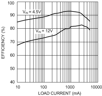
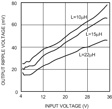
8.2.3 Application Curves

| VOUT = 3.3 V | L = 6.8 µH |

| VOUT = 3.3 V | IOUT = 1 A | COUT(ESR) = 80 mΩ |
| Cff = 100 pF |