SNVS089O July 2000 – July 2015 LM3488
PRODUCTION DATA.
- 1 Features
- 2 Applications
- 3 Description
- 4 Revision History
- 5 Pin Configuration and Functions
- 6 Specifications
- 7 Detailed Description
-
8 Application and Implementation
- 8.1 Application Information
- 8.2
Typical Applications
- 8.2.1
Boost Converter
- 8.2.1.1 Design Requirements
- 8.2.1.2
Detailed Design Procedure
- 8.2.1.2.1 Custom Design with WEBENCH Tools
- 8.2.1.2.2 Power Inductor Selection
- 8.2.1.2.3 Programming the Output Voltage
- 8.2.1.2.4 Setting the Current Limit
- 8.2.1.2.5 Current Limit with External Slope Compensation
- 8.2.1.2.6 Power Diode Selection
- 8.2.1.2.7 Power MOSFET Selection
- 8.2.1.2.8 Input Capacitor Selection
- 8.2.1.2.9 Output Capacitor Selection
- 8.2.1.3 Application Curve
- 8.2.2 Designing SEPIC Using LM3488
- 8.2.1
Boost Converter
- 9 Power Supply Recommendations
- 10Layout
- 11Device and Documentation Support
- 12Mechanical, Packaging, and Orderable Information
Package Options
Mechanical Data (Package|Pins)
- DGK|8
Thermal pad, mechanical data (Package|Pins)
Orderable Information
8 Application and Implementation
NOTE
Information in the following applications sections is not part of the TI component specification, and TI does not warrant its accuracy or completeness. TI’s customers are responsible for determining suitability of components for their purposes. Customers should validate and test their design implementation to confirm system functionality.
8.1 Application Information
The LM3488 may be operated in either continuous or discontinuous conduction mode. The following applications are designed for continuous conduction operation. This mode of operation has higher efficiency and lower EMI characteristics than the discontinuous mode.
8.2 Typical Applications
8.2.1 Boost Converter
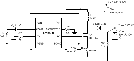 Figure 30. Typical High Efficiency Step-Up (Boost) Converter
The most common topology for LM3488 is the boost or step-up topology. The boost converter converts a low input voltage into a higher output voltage. The basic configuration for a boost regulator is shown in Figure 31. In continuous conduction mode (when the inductor current never reaches zero at steady state), the boost regulator operates in two cycles. In the first cycle of operation, MOSFET Q is turned on and energy is stored in the inductor. During this cycle, diode D is reverse biased and load current is supplied by the output capacitor, COUT.
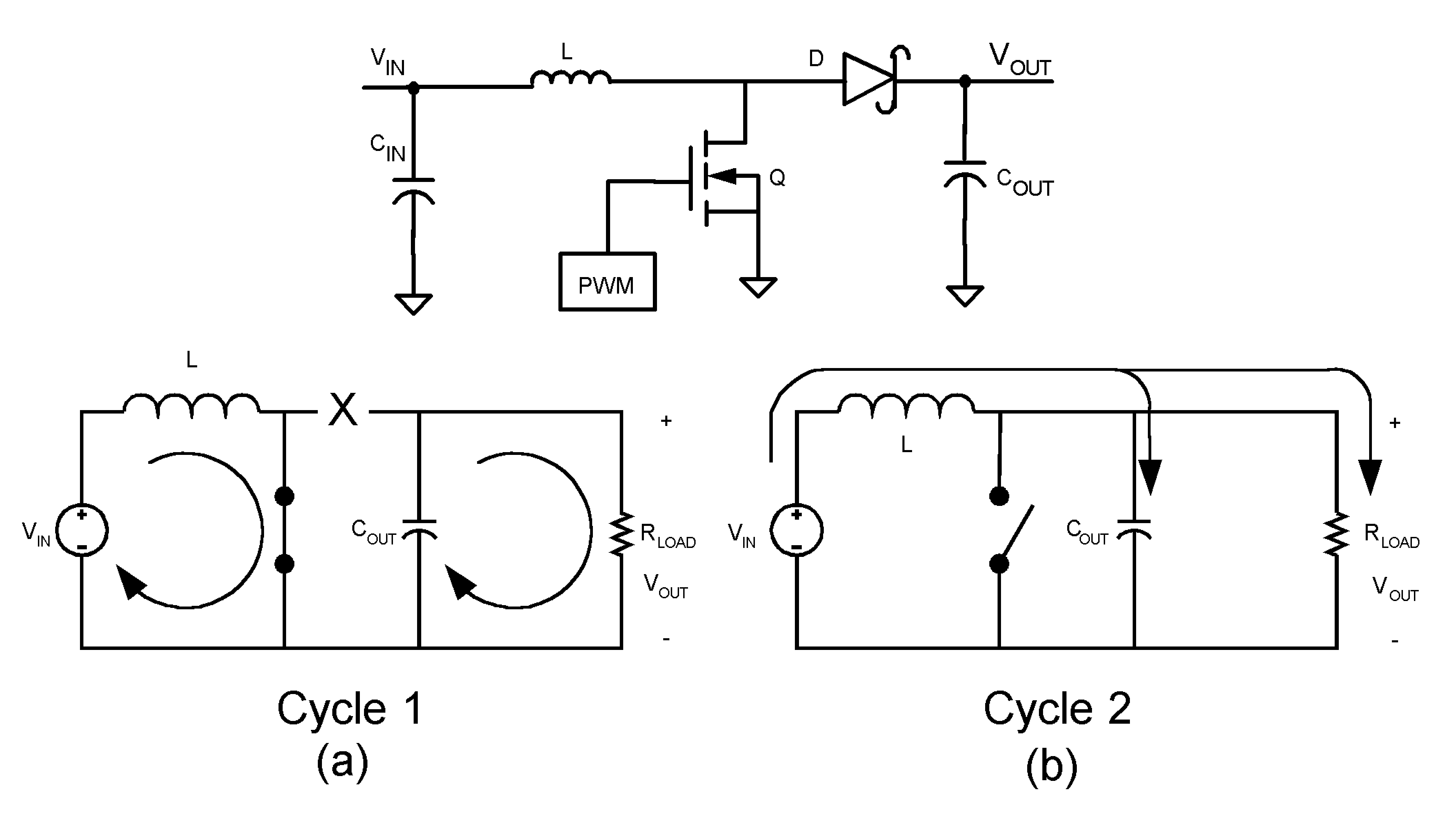 Figure 31. Simplified Boost Converter Diagram
(a) First cycle of operation
(b) Second cycle of operation
In the second cycle, MOSFET Q is off and the diode is forward biased. The energy stored in the inductor is transferred to the load and output capacitor. The ratio of these two cycles determines the output voltage. The output voltage is defined as:
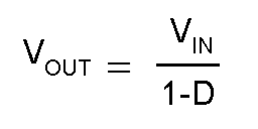
(ignoring the drop across the MOSFET and the diode), or
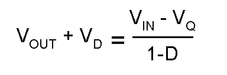
where
- D is the duty cycle of the switch
- VD is the forward voltage drop of the diode
- VQ is the drop across the MOSFET when it is on
8.2.1.1 Design Requirements
To calculate component values for a Boost converter, the power supply parameters shown in Table 2 should be known. The design shown in Figure 30 is the result of starting with example values shown in Table 2.
Table 2. Boost Design Parameters
| DESIGN PARAMETER | EXAMPLE VALUE |
|---|---|
| Input voltage range | 3V to 3.6V |
| Output voltage | 5V |
| Maximum current | 2A |
| Operating frequency | 350kHz |
8.2.1.2 Detailed Design Procedure
8.2.1.2.1 Custom Design with WEBENCH Tools
Click here to create a custom design using the LM3488 device with the WEBENCH® Power Designer.
- Start by entering your VIN, VOUT and IOUT requirements.
- Optimize your design for key parameters like efficiency, footprint and cost using the optimizer dial and compare this design with other possible solutions from Texas Instruments.
- WEBENCH Power Designer provides you with a customized schematic along with a list of materials with real time pricing and component availability.
- In most cases, you will also be able to:
- Run electrical simulations to see important waveforms and circuit performance,
- Run thermal simulations to understand the thermal performance of your board,
- Export your customized schematic and layout into popular CAD formats,
- Print PDF reports for the design, and share your design with colleagues.
- Get more information about WEBENCH tools at www.ti.com/webench.
8.2.1.2.2 Power Inductor Selection
The inductor is one of the two energy storage elements in a boost converter. Figure 32 shows how the inductor current varies during a switching cycle. The current through an inductor is quantified as:
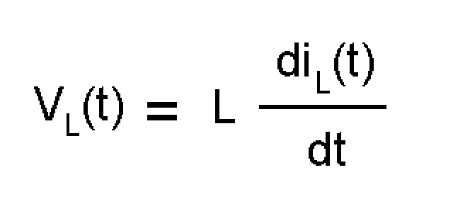
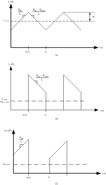 Figure 32. A. Inductor Current B. Diode Current C. Switch Current
If VL(t) is constant, diL(t)/dt must be constant. Hence, for a given input voltage and output voltage, the current in the inductor changes at a constant rate.
The important quantities in determining a proper inductance value are IL (the average inductor current) and ΔiL (the inductor current ripple). If ΔiL is larger than IL, the inductor current will drop to zero for a portion of the cycle and the converter will operate in discontinuous conduction mode. If ΔiL is smaller than IL, the inductor current will stay above zero and the converter will operate in continuous conduction mode. All the analysis in this datasheet assumes operation in continuous conduction mode. To operate in continuous conduction mode, the following conditions must be met:
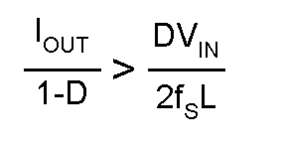
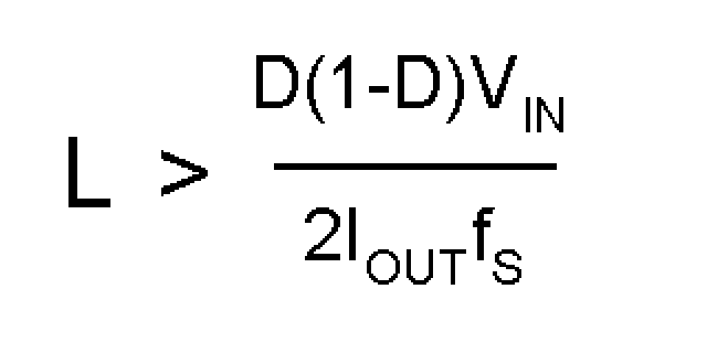
Choose the minimum IOUT to determine the minimum L. A common choice is to set ΔiL to 30% of IL. Choosing an appropriate core size for the inductor involves calculating the average and peak currents expected through the inductor. In a boost converter,
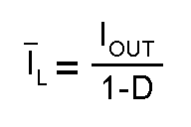
and IL_peak = IL(max) + ΔiL(max),
where

A core size with ratings higher than these values should be chosen. If the core is not properly rated, saturation will dramatically reduce overall efficiency.
The LM3488 can be set to switch at very high frequencies. When the switching frequency is high, the converter can be operated with very small inductor values. With a small inductor value, the peak inductor current can be extremely higher than the output currents, especially under light load conditions.
The LM3488 senses the peak current through the switch. The peak current through the switch is the same as the peak current calculated above.
8.2.1.2.3 Programming the Output Voltage
The output voltage can be programmed using a resistor divider between the output and the feedback pins, as shown in Figure 33. The resistors are selected such that the voltage at the feedback pin is 1.26V. RF1 and RF2 can be selected using the equation,

A 100-pF capacitor may be connected between the feedback and ground pins to reduce noise.
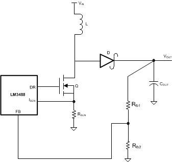 Figure 33. Adjusting the Output Voltage
8.2.1.2.4 Setting the Current Limit
The maximum amount of current that can be delivered to the load is set by the sense resistor, RSEN. Current limit occurs when the voltage that is generated across the sense resistor equals the current sense threshold voltage, VSENSE. When this threshold is reached, the switch will be turned off until the next cycle. Limits for VSENSE are specified in Electrical Characteristics. VSENSE represents the maximum value of the internal control signal VCS. This control signal, however, is not a constant value and changes over the course of a period as a result of the internal compensation ramp (see Figure 20). Therefore the current limit threshold will also change. The actual current limit threshold is a function of the sense voltage (VSENSE) and the internal compensation ramp:
where
- ISWLIMIT is the peak switch current limit, defined by the equation below. As duty cycle increases, the control voltage is reduced as VSL ramps up. Since current limit threshold varies with duty cycle, the following equation should be used to select RSEN and set the desired current limit threshold:

The numerator of the above equation is VCS, and ISWLIMIT is calculated as:

To avoid false triggering, the current limit value should have some margin above the maximum operating value, typically 120%. Values for both VSENSE and VSL are specified in Electrical Characteristics. However, calculating with the limits of these two specs could result in an unrealistically wide current limit or RSEN range. Therefore, the following equation is recommended, using the VSL ratio value given in Electrical Characteristics:

RSEN is part of the current mode control loop and has some influence on control loop stability. Therefore, once the current limit threshold is set, loop stability must be verified. To verify stability, use the following equation:

If the selected RSEN is greater than this value, additional slope compensation must be added to ensure stability, as described in Current Limit with External Slope Compensation.
8.2.1.2.5 Current Limit with External Slope Compensation
RSL is used to add additional slope compensation when required. It is not necessary in most designs and RSL should be no larger than necessary. Select RSL according to the following equation:

where
- RSEN is the selected value based on current limit. With RSL installed, the control signal includes additional external slope to stabilize the loop, which will also have an effect on the current limit threshold. Therefore, the current limit threshold must be re-verified, as illustrated in the equations below :
where
- ΔVSL is the additional slope compensation generated and calculated as:
This changes the equation for current limit (or RSEN) to:

The RSEN and RSL values may have to be calculated iteratively in order to achieve both the desired current limit and stable operation. In some designs RSL can also help to filter noise on the ISEN pin.
If the inductor is selected such that ripple current is the recommended 30% value, and the current limit threshold is 120% of the maximum peak, a simpler method can be used to determine RSEN. The equation below will provide optimum stability without RSL, provided that the above 2 conditions are met:

8.2.1.2.6 Power Diode Selection
Observation of the boost converter circuit shows that the average current through the diode is the average load current, and the peak current through the diode is the peak current through the inductor. The diode should be rated to handle more than its peak current. The peak diode current can be calculated using the formula:
In the above equation, IOUT is the output current and ΔIL has been defined in Figure 32.
The peak reverse voltage for boost converter is equal to the regulator output voltage. The diode must be capable of handling this voltage. To improve efficiency, a low forward drop schottky diode is recommended.
8.2.1.2.7 Power MOSFET Selection
The drive pin of LM3488 must be connected to the gate of an external MOSFET. In a boost topology, the drain of the external N-Channel MOSFET is connected to the inductor and the source is connected to the ground. The drive pin (DR) voltage depends on the input voltage (see the Typical Characteristics section). In most applications, a logic level MOSFET can be used. For very low input voltages, a sub-logic level MOSFET should be used.
The selected MOSFET directly controls the efficiency. The critical parameters for selection of a MOSFET are:
- Minimum threshold voltage, VTH(MIN)
- On-resistance, RDS(ON)
- Total gate charge, Qg
- Reverse transfer capacitance, CRSS
- Maximum drain to source voltage, VDS(MAX)
The off-state voltage of the MOSFET is approximately equal to the output voltage. VDS(MAX) of the MOSFET must be greater than the output voltage. The power losses in the MOSFET can be categorized into conduction losses and ac switching or transition losses. RDS(ON) is needed to estimate the conduction losses. The conduction loss, PCOND, is the I2R loss across the MOSFET. The maximum conduction loss is given by:

where
- DMAX is the maximum duty cycle.

The turn-on and turn-off transitions of a MOSFET require times of tens of nano-seconds. CRSS and Qg are needed to estimate the large instantaneous power loss that occurs during these transitions.
The amount of gate current required to turn the MOSFET on can be calculated using the formula:
The required gate drive power to turn the MOSFET on is equal to the switching frequency times the energy required to deliver the charge to bring the gate charge voltage to VDR (see the Electrical Characteristics table and the Typical Characteristics section for the drive voltage specification).
8.2.1.2.8 Input Capacitor Selection
Due to the presence of an inductor at the input of a boost converter, the input current waveform is continuous and triangular, as shown in Figure 32. The inductor ensures that the input capacitor sees fairly low ripple currents. However, as the input capacitor gets smaller, the input ripple goes up. The rms current in the input capacitor is given by:

The input capacitor should be capable of handling the rms current. Although the input capacitor is not as critical in a boost application, low values can cause impedance interactions. Therefore a good quality capacitor should be chosen in the range of 10 µF to 20 µF. If a value lower than 10µF is used, then problems with impedance interactions or switching noise can affect the LM3488. To improve performance, especially with VIN below 8 volts, it is recommended to use a 20Ω resistor at the input to provide a RC filter. The resistor is placed in series with the VIN pin with only a bypass capacitor attached to the VIN pin directly (see Figure 34). A 0.1-µF or 1-µF ceramic capacitor is necessary in this configuration. The bulk input capacitor and inductor will connect on the other side of the resistor with the input power supply.
 Figure 34. Reducing IC Input Noise
8.2.1.2.9 Output Capacitor Selection
The output capacitor in a boost converter provides all the output current when the inductor is charging. As a result it sees very large ripple currents. The output capacitor should be capable of handling the maximum rms current. The rms current in the output capacitor is:

Where
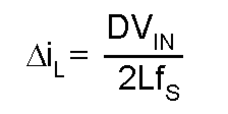
and D, the duty cycle is equal to (VOUT − VIN)/VOUT.
The ESR and ESL of the output capacitor directly control the output ripple. Use capacitors with low ESR and ESL at the output for high efficiency and low ripple voltage. Surface Mount tantalums, surface mount polymer electrolytic and polymer tantalum, Sanyo- OSCON, or multi-layer ceramic capacitors are recommended at the output.
8.2.1.3 Application Curve
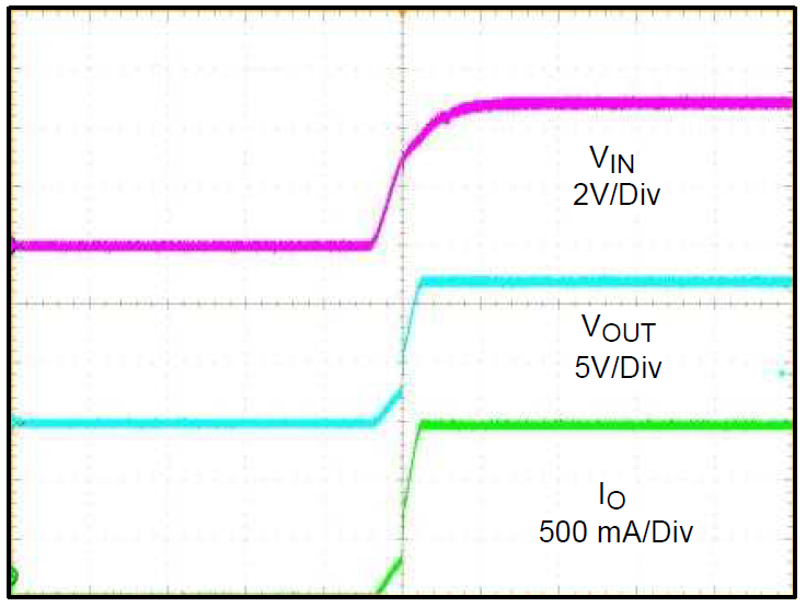 Figure 35. Typical Startup Waveform (horizontal scale: 10ms/DIV)
8.2.2 Designing SEPIC Using LM3488
Since the LM3488 controls a low-side N-Channel MOSFET, it can also be used in SEPIC (Single Ended Primary Inductance Converter) applications. An example of SEPIC using LM3488 is shown in Figure 36. As shown in Figure 36, the output voltage can be higher or lower than the input voltage. The SEPIC uses two inductors to step-up or step-down the input voltage. The inductors L1 and L2 can be two discrete inductors or two windings of a coupled transformer since equal voltages are applied across the inductor throughout the switching cycle. Using two discrete inductors allows use of catalog magnetics, as opposed to a custom transformer. The input ripple can be reduced along with size by using the coupled windings of transformer for L1 and L2.
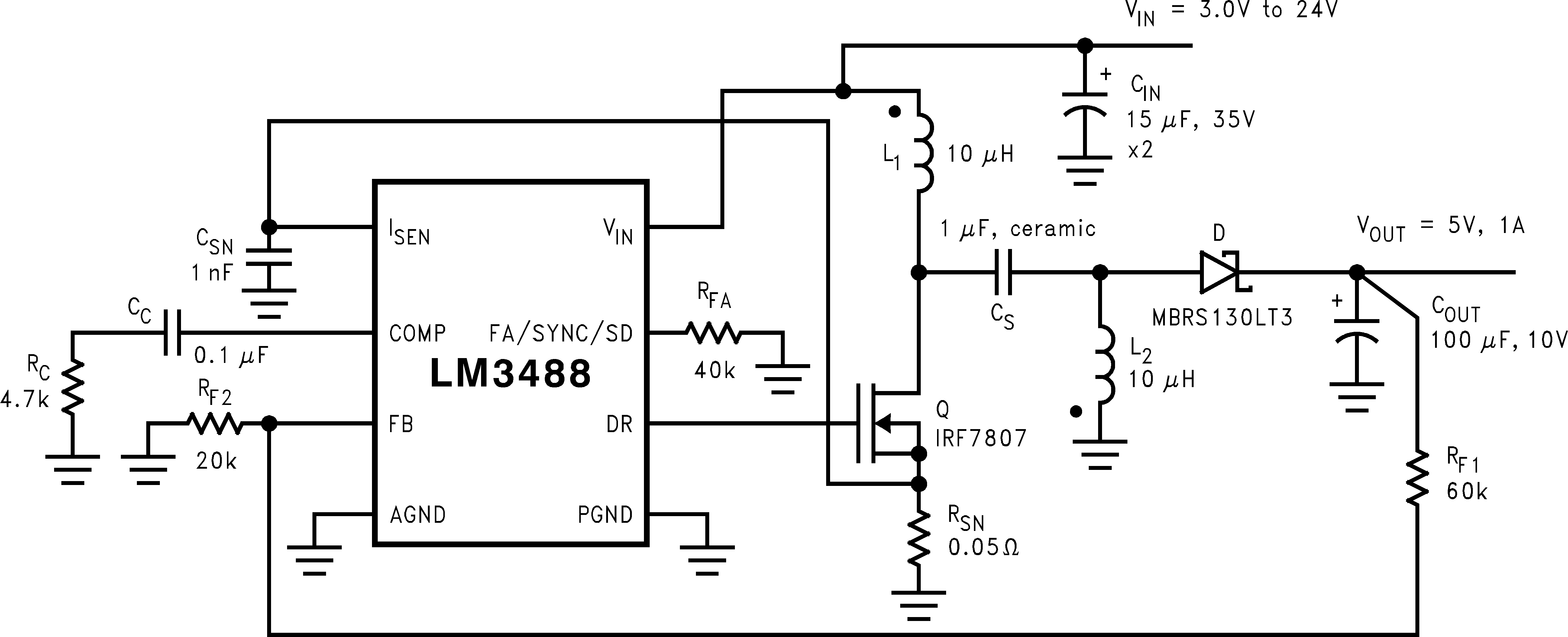 Figure 36. Typical SEPIC Converter
Due to the presence of the inductor L1 at the input, the SEPIC inherits all the benefits of a boost converter. One main advantage of SEPIC over boost converter is the inherent input to output isolation. The capacitor CS isolates the input from the output and provides protection against shorted or malfunctioning load. Hence, the A SEPIC is useful for replacing boost circuits when true shutdown is required. This means that the output voltage falls to 0V when the switch is turned off. In a boost converter, the output can only fall to the input voltage minus a diode drop.
The duty cycle of a SEPIC is given by:

In the above equation, VQ is the on-state voltage of the MOSFET, Q, and VDIODE is the forward voltage drop of the diode.
8.2.2.1 Design Requirements
To calculate component values for a SEPIC converter, the power supply parameters shown in Table 3 should be known. The design shown in Figure 36 is the result of starting with example values shown in Table 3
Table 3. SEPIC Design Parameters
| DESIGN PARAMETER | EXAMPLE VALUE |
|---|---|
| Input voltage range | 3 V to 24 V |
| Output voltage | 5 V |
| Maximum current | 1 A |
| Operating frequency | 350 kHz |
| Max peak to peak output ripple | 200 mV |
8.2.2.2 Detailed Design Procedure
8.2.2.2.1 Power MOSFET Selection
As in boost converter, the parameters governing the selection of the MOSFET are the minimum threshold voltage, VTH(MIN), the on-resistance, RDS(ON), the total gate charge, Qg, the reverse transfer capacitance, CRSS, and the maximum drain to source voltage, VDS(MAX). The peak switch voltage in a SEPIC is given by:
The selected MOSFET should satisfy the condition:
The peak switch current is given by:

The rms current through the switch is given by:

8.2.2.2.2 Power Diode Selection
The Power diode must be selected to handle the peak current and the peak reverse voltage. In a SEPIC, the diode peak current is the same as the switch peak current. The off-state voltage or peak reverse voltage of the diode is VIN + VOUT. Similar to the boost converter, the average diode current is equal to the output current. Schottky diodes are recommended.
8.2.2.2.3 Selection Of Inductors L1 and L2
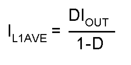
Proper selection of the inductors L1 and L2 to maintain constant current mode requires calculations of the following parameters.
Average current in the inductors:
Peak to peak ripple current, to calculate core loss if necessary:
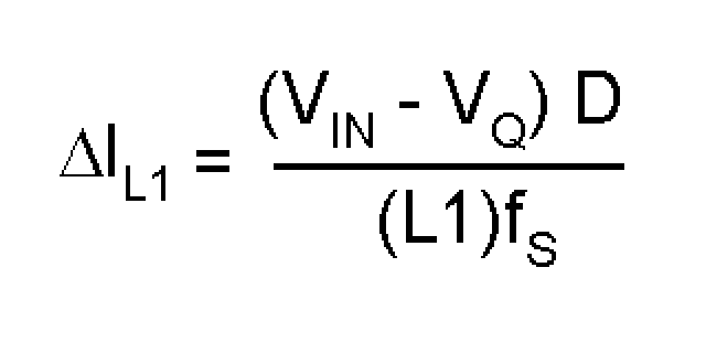
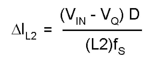
maintains the condition IL > ΔiL/2 to ensure constant current mode.


Peak current in the inductor, to ensure the inductor does not saturate:

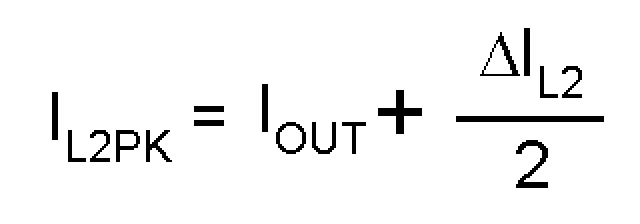
IL1PK must be lower than the maximum current rating set by the current sense resistor.
The value of L1 can be increased above the minimum recommended to reduce input ripple and output ripple. However, once DIL1 is less than 20% of IL1AVE, the benefit to output ripple is minimal.
By increasing the value of L2 above the minimum recommended, ΔIL2 can be reduced, which in turn will reduce the output ripple voltage:

where
- ESR is the effective series resistance of the output capacitor.
If L1 and L2 are wound on the same core, then L1 = L2 = L. All the equations above will hold true if the inductance is replaced by 2L. A good choice for transformer with equal turns is Coiltronics CTX series Octopack.
8.2.2.2.4 Sense Resistor Selection
The peak current through the switch, ISW(PEAK) can be adjusted using the current sense resistor, RSEN, to provide a certain output current. Resistor RSEN can be selected using the formula:

8.2.2.2.5 SEPIC Capacitor Selection
The selection of SEPIC capacitor, CS, depends on the rms current. The rms current of the SEPIC capacitor is given by:

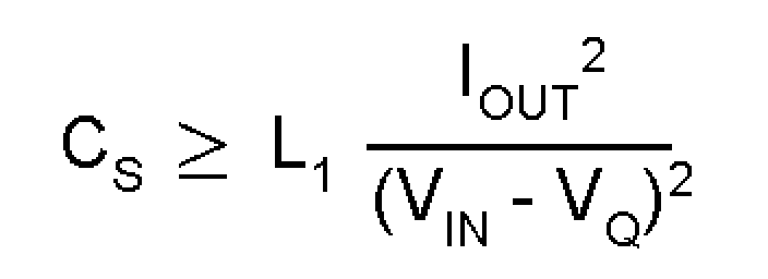
The SEPIC capacitor must be rated for a large ACrms current relative to the output power. This property makes the SEPIC much better suited to lower power applications where the rms current through the capacitor is relatively small (relative to capacitor technology). The voltage rating of the SEPIC capacitor must be greater than the maximum input voltage. Tantalum capacitors are the best choice for SMT, having high rms current ratings relative to size. Ceramic capacitors could be used, but the low C values will tend to cause larger changes in voltage across the capacitor due to the large currents. High C value ceramics are expensive. Electrolytics work well for through hole applications where the size required to meet the rms current rating can be accommodated. There is an energy balance between CS and L1, which can be used to determine the value of the capacitor. The basic energy balance equation is:

Where

is the ripple voltage across the SEPIC capacitor, and
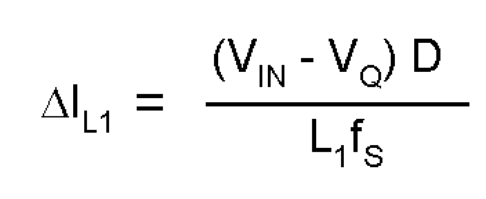
is the ripple current through the inductor L1. The energy balance equation can be solved to provide a minimum value for CS:
8.2.2.2.6 Input Capacitor Selection
Similar to a boost converter, the SEPIC has an inductor at the input. Hence, the input current waveform is continuous and triangular. The inductor ensures that the input capacitor sees fairly low ripple currents. However, as the input capacitor gets smaller, the input ripple goes up. The rms current in the input capacitor is given by:

The input capacitor should be capable of handling the rms current. Although the input capacitor is not as critical in a boost application, low values can cause impedance interactions. Therefore a good quality capacitor should be chosen in the range of 10µF to 20µF. If a value lower than 10µF is used, then problems with impedance interactions or switching noise can affect the LM3488. To improve performance, especially with VIN below 8 volts, it is recommended to use a 20Ω resistor at the input to provide a RC filter. The resistor is placed in series with the VIN pin with only a bypass capacitor attached to the VIN pin directly (see Figure 34). A 0.1µF or 1µF ceramic capacitor is necessary in this configuration. The bulk input capacitor and inductor will connect on the other side of the resistor with the input power supply.
8.2.2.2.7 Output Capacitor Selection
The ESR and ESL of the output capacitor directly control the output ripple. Use low capacitors with low ESR and ESL at the output for high efficiency and low ripple voltage. Surface mount tantalums, surface mount polymer electrolytic and polymer tantalum, Sanyo- OSCON, or multi-layer ceramic capacitors are recommended at the output.
The output capacitor of the SEPIC sees very large ripple currents (similar to the output capacitor of a boost converter. The rms current through the output capacitor is given by:

The ESR and ESL of the output capacitor directly control the output ripple. Use low capacitors with low ESR and ESL at the output for high efficiency and low ripple voltage. Surface mount tantalums, surface mount polymer electrolytic and polymer tantalum, Sanyo- OSCON, or multi-layer ceramic capacitors are recommended at the output for low ripple.