SNVS797B March 2012 – October 2015 LM3492HC , LM3492HC-Q1
PRODUCTION DATA.
- 1 Features
- 2 Applications
- 3 Description
- 4 Revision History
- 5 Description (continued)
- 6 Pin Configuration and Functions
- 7 Specifications
-
8 Detailed Description
- 8.1 Overview
- 8.2 Functional Block Diagram
- 8.3 Feature Description
- 8.4 Device Functional Modes
- 8.5 Programming
- 9 Application and Implementation
- 10Power Supply Recommendations
- 11Layout
- 12Device and Documentation Support
- 13Mechanical, Packaging, and Orderable Information
Package Options
Mechanical Data (Package|Pins)
- PWP|20
Thermal pad, mechanical data (Package|Pins)
- PWP|20
Orderable Information
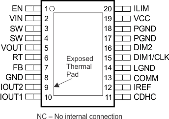
6 Pin Configuration and Functions
PWP Package
20 Pin HTSSOP
Top View

Pin Functions
| PIN | TYPE(1) | DESCRIPTION | |
|---|---|---|---|
| NAME | NO. | ||
| CDHC | 11 | I | Dynamic headroom control. An external capacitor connected to this pin sets the DHC sensitivity. At start-up, a 12- µA internal current source charges an external capacitor to provide a soft-start function. |
| COMM | 13 | I/O | Bidirectional logic communication. This pin is open drain for various indications (power-good, overtemperature, IOUT overvoltage and undervoltage) and command sending (switching frequency tuning and channel 1 disabling). |
| DIM1/CLK | 15 | I/O | Dimming control of channel 1. Control the on and off of the current regulator of channel 1. This pin is internally pulled low by a 5-µA current. This pin also serves as a clock signal for latching input and output data of the COMM pin. |
| DIM2 | 16 | I | Dimming control of channel 2. Control the on and off of the current regulator of channel 2. This pin is internally pulled low by a 5-µA current. |
| EN | 1 | I | Enable input. Contains an internal pullup. Connect to a voltage higher than 1.63 V to provide precision enable for the device. |
| FB | 7 | I | Output voltage feedback. The output voltage is connected to this pin through a feedback resistor divider for output voltage regulation. The voltage of this pin is from 1.05 V to 2.5 V. |
| GND | 8 | G | Analog signal ground. Connect to the exposed pad directly beneath the device. |
| ILIM | 20 | I | Peak current limit adjust. Connecting an external resistor from the ILIM pin to the VCC pin reduces peak current limit. Connect the ILIM pin to ground to obtain the maximum current limit. |
| IOUT1 | 10 | I | Current regulator input for channel 1. Input of the current regulator of channel 1. The regulated current is programmable (see the IREF pin). |
| IOUT2 | 9 | I | Current regulator input for channel 2. Input of the current regulator of channel 2. The regulated current is programmable (see the IREF pin). |
| IREF | 12 | I | Current setting pin for the current regulators. An external resistor connected from this pin to ground programs the regulated current of the current regulator of channels 1 and 2. |
| LGND | 14 | G | Current regulator ground. Must be connected to the GND pin and exposed pad for normal operation. The LGND and GND pins are not internally connected. |
| PGND | 17 | G | Integrated MOSFET ground. Must be connected to the GND pin and exposed pad for normal operation. The PGND and GND pins are not internally connected. |
| 18 | |||
| RT | 6 | I | Frequency control pin. An external resistor from the VOUT pin to this pin sets the switching frequency. |
| SW | 3 | I | Switch node. Internally connected to the drain of the integrated MOSFET. |
| 4 | |||
| VCC | 19 | O | Internal LED regulator output. Nominally regulated to 5.5 V. Connect a capacitor of 0.47-μF or larger between the VCC and GND pins. |
| VIN | 2 | I | Input supply voltage pin. Input voltage range is from 4.5 V to 65 V. |
| VOUT | 5 | I | Output voltage sense pin. Senses the output voltage for nearly constant switching frequency control. |
| Exposed Pad | G | Thermal connection pad. Connect to a ground plane. | |
(1) I = Input, O = Output, G = Ground