SNVS569C May 2009 – October 2016 LM3550
PRODUCTION DATA.
- 1 Features
- 2 Applications
- 3 Description
- 4 Revision History
- 5 Pin Configuration and Functions
- 6 Specifications
-
7 Detailed Description
- 7.1 Overview
- 7.2 Functional Block Diagram
- 7.3 Feature Description
- 7.4 Device Functional Modes
- 7.5 Programming
- 7.6 Register Maps
- 8 Application and Implementation
- 9 Power Supply Recommendations
- 10Layout
- 11Device and Documentation Support
- 12Mechanical, Packaging, and Orderable Information
Package Options
Mechanical Data (Package|Pins)
- NHU|20
Thermal pad, mechanical data (Package|Pins)
Orderable Information
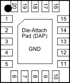
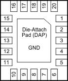
5 Pin Configuration and Functions
NHU Package
16-Pin UQFN
Top View

NHU Package
16-Pin UQFN
Bottom View

Pin Functions
| PIN | TYPE | DESCRIPTION | |
|---|---|---|---|
| NAME | NUMBER | ||
| ALD/TEMP | 12 | Input | Ambient light sensor or temperature monitoring pin. For ambient light sensing, connect a light sensor or photo-diode and a resistor to this pin. For temperature monitoring, connect a NTC thermistor from VCC to the NTC pin and a resistor from the NTC pin to ground. |
| BAL | 2 | Power | Super-capacitor active balance pin |
| C1+ | 20 | Power | Flying capacitor pins. Connect a 1-µF ceramic capacitor from C1+ to C1− and C2+ to C2−. |
| C1– | 18 | ||
| C2+ | 15 | ||
| C2– | 16 | ||
| EOC | 6 | Output | End-of-charge output/ flash ready. The EOC pin transitions from high to low when an end of charge flash ready. The EOC pin transitions from high to low when an end of charge state has been reached |
| FB | 5 | Input | Programmable feedback voltage pin |
| FET_CON | 4 | Output | External FET controller. Connect gate of flash NFET to this pin. |
| IND | 13 | Output | Indicator LED current source. Drives one red LED with a 5-mA current |
| LED- | 3 | Input | Regulated current sink input for torch mode |
| SCL | 10 | Input | I2C serial clock pin |
| SDA | 8 | Input/Output | I2C serial data I/O pin |
| STROBE | 11 | Input | Manual flash enable pin. The STROBE pin can be configured to be rising-edge sensitive with the flash timing controlled internally, or level sensitive with the flash timing being controlled externally. |
| VIN | 14 | Input | Input voltage connection. A 1-μF ceramic capacitor is required from VIN to GND. |
| VOUT | 1 | Output | Charge pump output. A 1-μF ceramic capacitor is required from VOUT to GND. Connect the flash LED anodes and super-capacitor to this pin. |
| GND | 7,9,17,19, DAP | Ground | Ground pins – these pins should be connected directly to a low-impedance ground plane. |