SNVS549C June 2009 – February 2016 LM3554
PRODUCTION DATA.
- 1 Features
- 2 Applications
- 3 Description
- 4 Revision History
- 5 Specifications
-
6 Detailed Description
- 6.1 Overview
- 6.2 Functional Block Diagram
- 6.3
Feature Description
- 6.3.1 Start-Up
- 6.3.2 Overvoltage Protection
- 6.3.3 Current Limit
- 6.3.4 Flash Termination (Strobe-Initiated Flash)
- 6.3.5 Flash Termination (I2C-Initiated Flash)
- 6.3.6 Flash Timeout
- 6.3.7 Torch Mode
- 6.3.8 TX1/Torch
- 6.3.9 ENVM/TX2/GPIO2
- 6.3.10 Indicator LED/Thermistor (LEDI/NTC)
- 6.3.11 Alternative External Torch (AET Mode)
- 6.3.12 Input Voltage Monitor
- 6.3.13 LM3554 Timing Diagrams
- 6.3.14 Flags Register and Fault Indicators
- 6.3.15 Thermal Shutdown
- 6.3.16 LED Fault
- 6.3.17 Flash Timeout
- 6.3.18 LED Thermal Fault
- 6.3.19 Input Voltage Monitor Fault
- 6.3.20 TX1 And TX2 Interrupt Flags
- 6.3.21 Light Load Disable
- 6.4 Device Functional Modes
- 6.5 Programming
- 6.6 Register Maps
-
7 Application and Implementation
- 7.1 Application Information
- 7.2
Typical Application
- 7.2.1 Design Requirements
- 7.2.2 Detailed Design Procedure
- 7.2.3 Application Curves
- 8 Power Supply Recommendations
- 9 Layout
- 10Device and Documentation Support
- 11Mechanical, Packaging, and Orderable Information
Package Options
Mechanical Data (Package|Pins)
- YFQ|16
Thermal pad, mechanical data (Package|Pins)
Orderable Information
5 Specifications
5.1 Absolute Maximum Ratings
over operating free-air temperature range (unless otherwise noted)(1)(2)(3)| MIN | MAX | UNIT | ||
|---|---|---|---|---|
| VIN, VSW, VOUT | –0.3 | 6 | V | |
| VSCL, VSDA, VHWEN, VSTROBE, VTX1/TORCH, VENVM/TX2, VLED1, VLED2, VLEDI/NTC | 0.3 V to (VIN + 0.3 V) w/ 6 V max |
|||
| Continuous power dissipation(4) | Internally limit | |||
| Junction temperature, TJ-MAX | 150 | °C | ||
| Maximum lead temperature (soldering) | See(5) | |||
| Storage temperature, Tstg | –65 | 150 | °C | |
(1) Stresses beyond those listed under Absolute Maximum Ratings may cause permanent damage to the device. These are stress ratings only, which do not imply functional operation of the device at these or any other conditions beyond those indicated under Recommended Operating Conditions. Exposure to absolute-maximum-rated conditions for extended periods may affect device reliability.
(2) All voltages are with respect to the potential at the GND pin.
(3) If Military/Aerospace specified devices are required, contact the Texas Instruments Sales Office/ Distributors for availability and specifications.
(4) Internal thermal shutdown circuitry protects the device from permanent damage. Thermal shutdown engages at TJ=150°C (typical) and disengages at TJ=135°C (typical).
(5) For detailed soldering specifications and information, refer to AN1112 DSBGA Wafer Level Chip-Scale Package (SNVA009).
5.2 ESD Ratings
| VALUE | UNIT | |||
|---|---|---|---|---|
| V(ESD) | Electrostatic discharge | Human-body model (HBM), per ANSI/ESDA/JEDEC JS-001(1) | ±2000 | V |
(1) JEDEC document JEP155 states that 500-V HBM allows safe manufacturing with a standard ESD control process.
5.3 Recommended Operating Conditions
over operating free-air temperature range (unless otherwise noted)(1)| MIN | NOM | MAX | UNIT | ||
|---|---|---|---|---|---|
| Input voltage, VIN | 2.5 | 5.5 | V | ||
| Junction temperature, TJ | –30 | 125 | °C | ||
| Ambient temperature, TA(2) | –30 | 85 | °C | ||
(1) All voltages are with respect to the potential at the GND pin.
(2) In applications where high power dissipation and/or poor package thermal resistance is present, the maximum ambient temperature may have to be derated. Maximum ambient temperature (TA-MAX) is dependent on the maximum operating junction temperature (TJ-MAX-OP = 125°C), the maximum power dissipation of the device in the application (PD-MAX), and the junction-to-ambient thermal resistance of the part/package in the application (RθJA), as given by the following equation: TA-MAX = TJ-MAX-OP – (RθJA × PD-MAX).
5.4 Thermal Information
| THERMAL METRIC(1) | LM3554 | UNIT | |
|---|---|---|---|
| YFQ (DSBGA) | |||
| 16 PINS | |||
| RθJA | Junction-to-ambient thermal resistance | 75.8 | °C/W |
| RθJC(top) | Junction-to-case (top) thermal resistance | 0.5 | °C/W |
| RθJB | Junction-to-board thermal resistance | 16.5 | °C/W |
| ψJT | Junction-to-top characterization parameter | 0.3 | °C/W |
| ψJB | Junction-to-board characterization parameter | 16.4 | °C/W |
(1) For more information about traditional and new thermal metrics, see the Semiconductor and IC Package Thermal Metrics application report, SPRA953.
5.5 Electrical Characteristics
Unless otherwise specified, typical limits are for TA = 25°C, minimum and maximum limits in apply over the full operating ambient temperature range (–30°C ≤ TA ≤ +85°C), VIN = 3.6 V, and VHWEN = VIN. (1)(2)| PARAMETER | TEST CONDITIONS | MIN | TYP | MAX | UNIT | ||
|---|---|---|---|---|---|---|---|
| CURRENT SOURCE SPECIFICATIONS | |||||||
| ILED | Current source accuracy | 600-mA flash LED setting, VOUT = VIN | ILED1 and ILED2 | 1128 | 1200 | 1284 | mA |
| ILED1 or ILED2 | 541 | 600 | 657 | ||||
| 17-mA torch current setting VHR = 500 mV |
ILED1 and ILED2 | 30.4 | 33.8 | 37.2 | |||
| VHR | Current source regulation voltage (VOUT – VLED) | 600-mA setting, VOUT = 3.75 V | 300 | mV | |||
| IMATCH | LED Current Matching | 600-mA setting, VLED = 3.2 V | 0.35% | ||||
| STEP-UP DC-DC CONVERTER | |||||||
| VREG | Output voltage accuracy | 2.7 V ≤ VIN ≤ 4.2 V, IOUT = 0 mA VENVM = VIN, OV bit = 0 |
4.8 | 5 | 5.2 | V | |
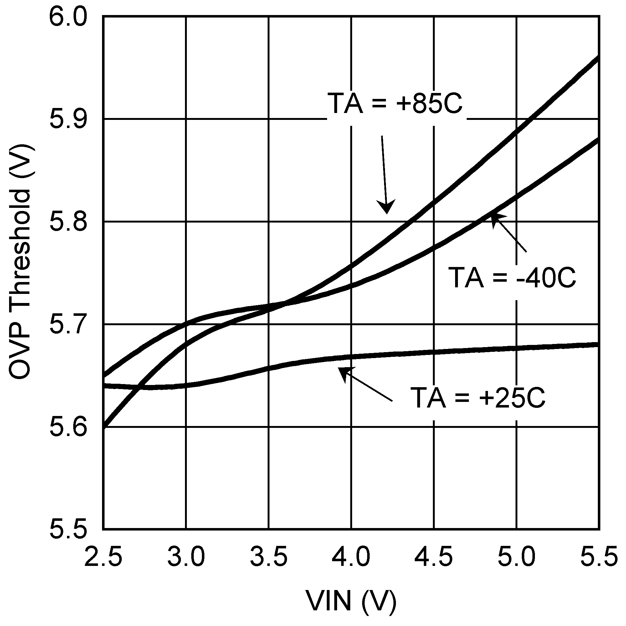
| VOVP | Output overvoltage protection trip point(3) | On threshold, 2.7 V ≤ VIN ≤ 5.5 V | 5.4 | 5.6 | 5.7 | V | |
| Off threshold | 5.3 | ||||||
| RPMOS | PMOS switch on-resistance | IPMOS = 1 A | 150 | mΩ | |||
| RNMOS | NMOS switch on-resistance | INMOS = 1 A | 150 | mΩ | |||
| ICL | Switch current limit(4) | CL bits = 00 | 0.711 | 1.05 | 1.373 | A | |
| CL bits = 01 | 1.295 | 1.51 | 1.8 | ||||
| CL bits = 10 | 1.783 | 1.99 | 2.263 | ||||
| CL bits = 11 | 2.243 | 2.45 | 2.828 | ||||
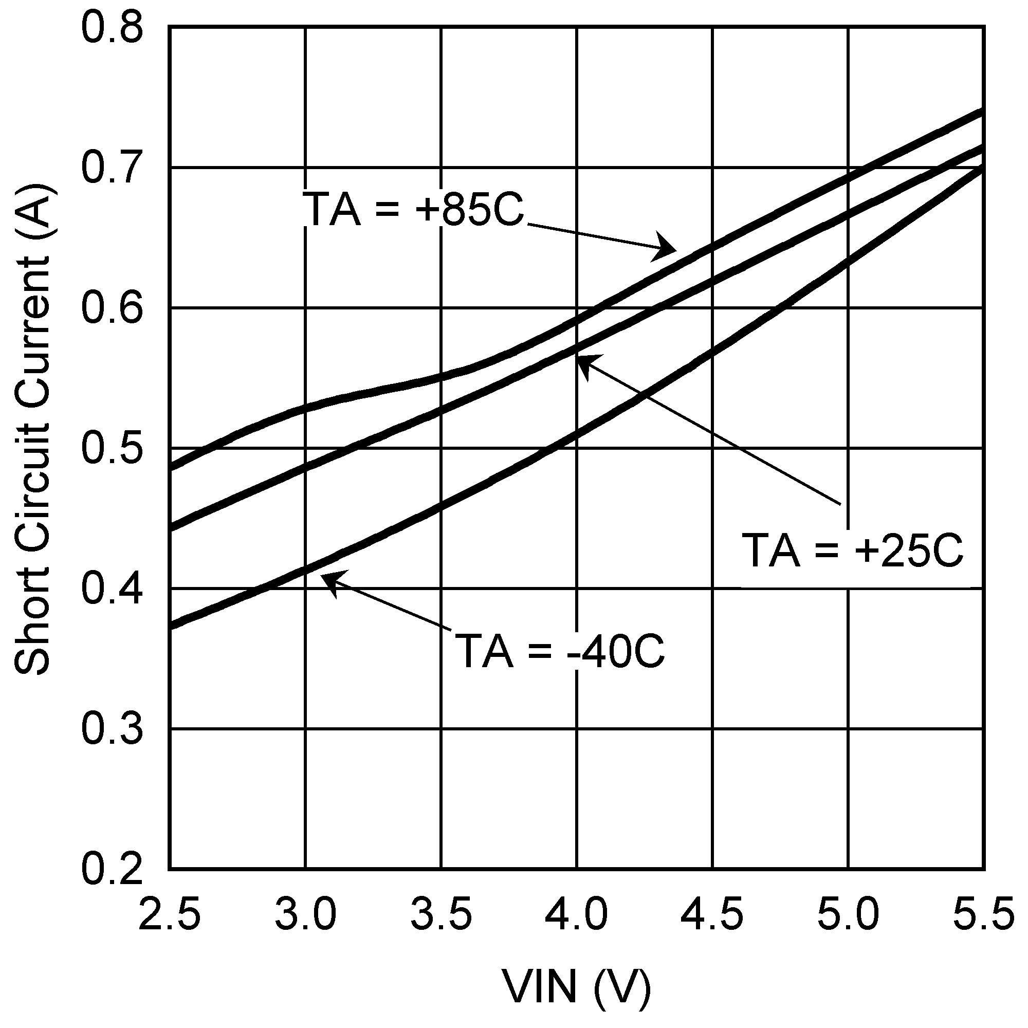
| IOUT_SC | Output short-circuit current limit | VOUT < 2.3 V | 550 | mA | |||
| ILED/NTC | Indicator current | LEDI/NTC bit = 0 | IND1, IND0 bits = 00 | 2.3 | mA | ||
| IND1, IND0 bits = 01 | 4.6 | ||||||
| IND1, IND0 bits = 10 | 6.9 | ||||||
| IND1, IND0 bits = 11 | 8.2 | ||||||
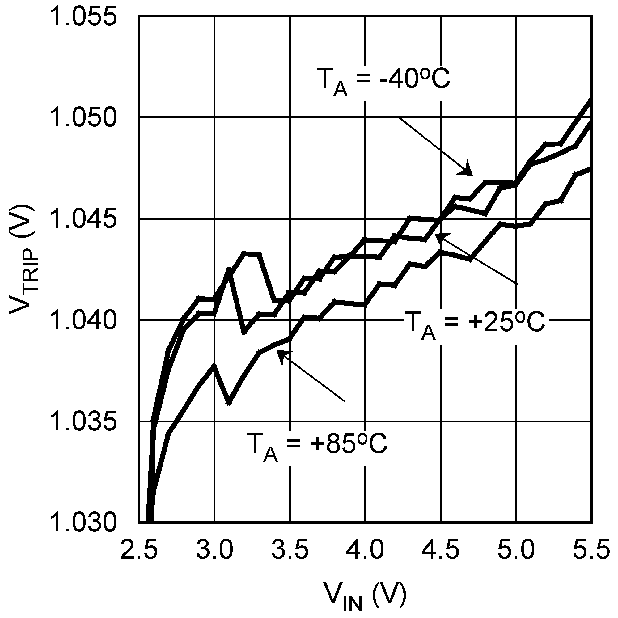
| VTRIP | Comparator trip threshold | LEDI/NTC bit = 1, 2.7 V ≤ VIN ≤ 5.5 V | 0.947 | 1.052 | 1.157 | V | |
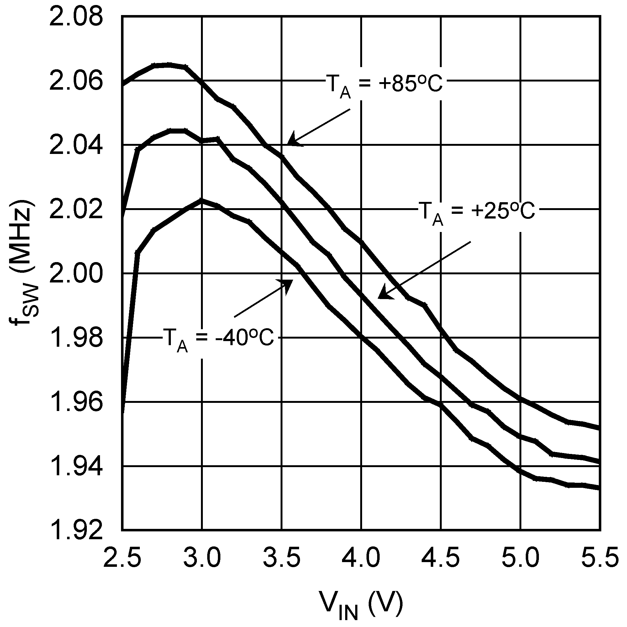
| ƒSW | Switching frequency | 2.7 V ≤ VIN ≤ 5.5 V | 1.75 | 2 | 2.23 | MHz | |
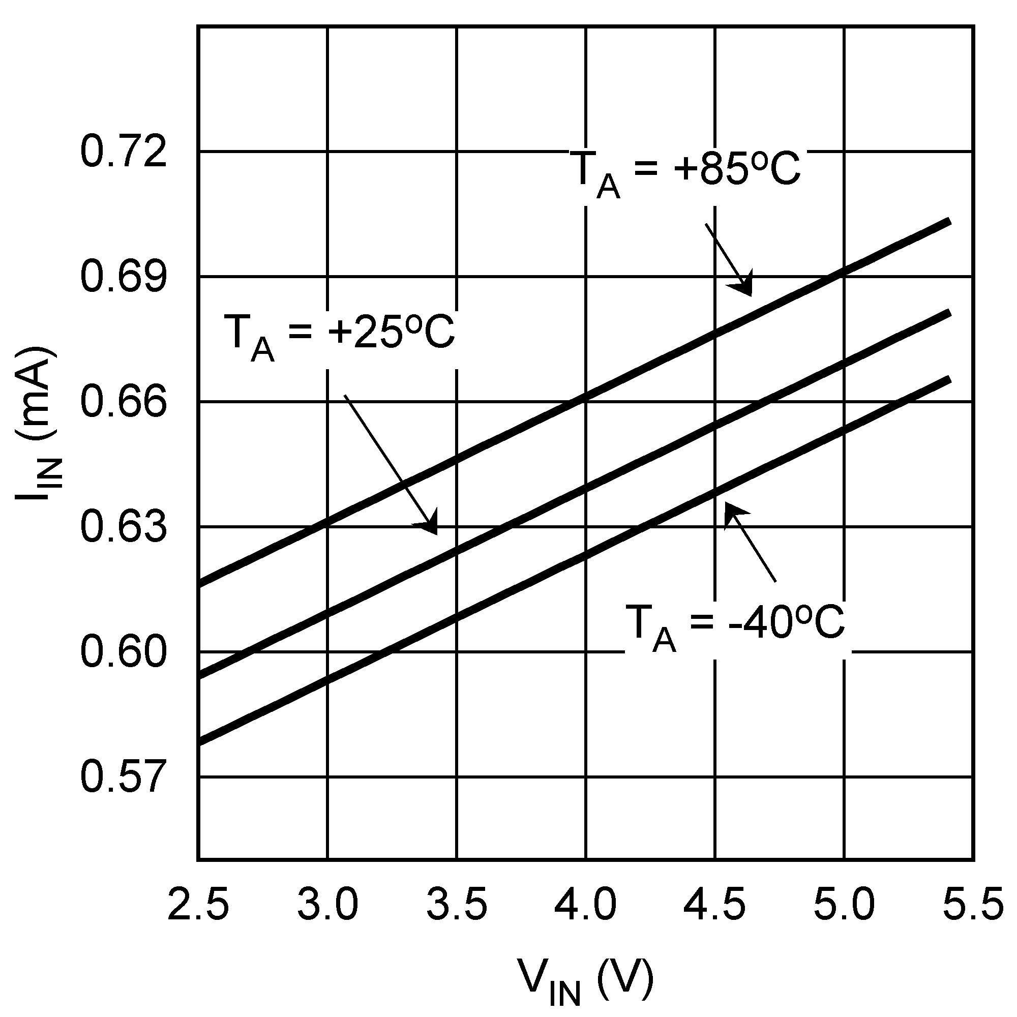
| IQ | Quiescent supply current | Device not switching | 630 | µA | |||
| ISHDN | Shutdown supply current | 2.7 V ≤ VIN ≤ 5.5 V | 3.5 | 6.6 | µA | ||
| tTX | Flash-to-torch LED current settling time | TX_ Low to High, ILED1 + ILED2 = 1.2 A to 180 mA | 20 | µs | |||
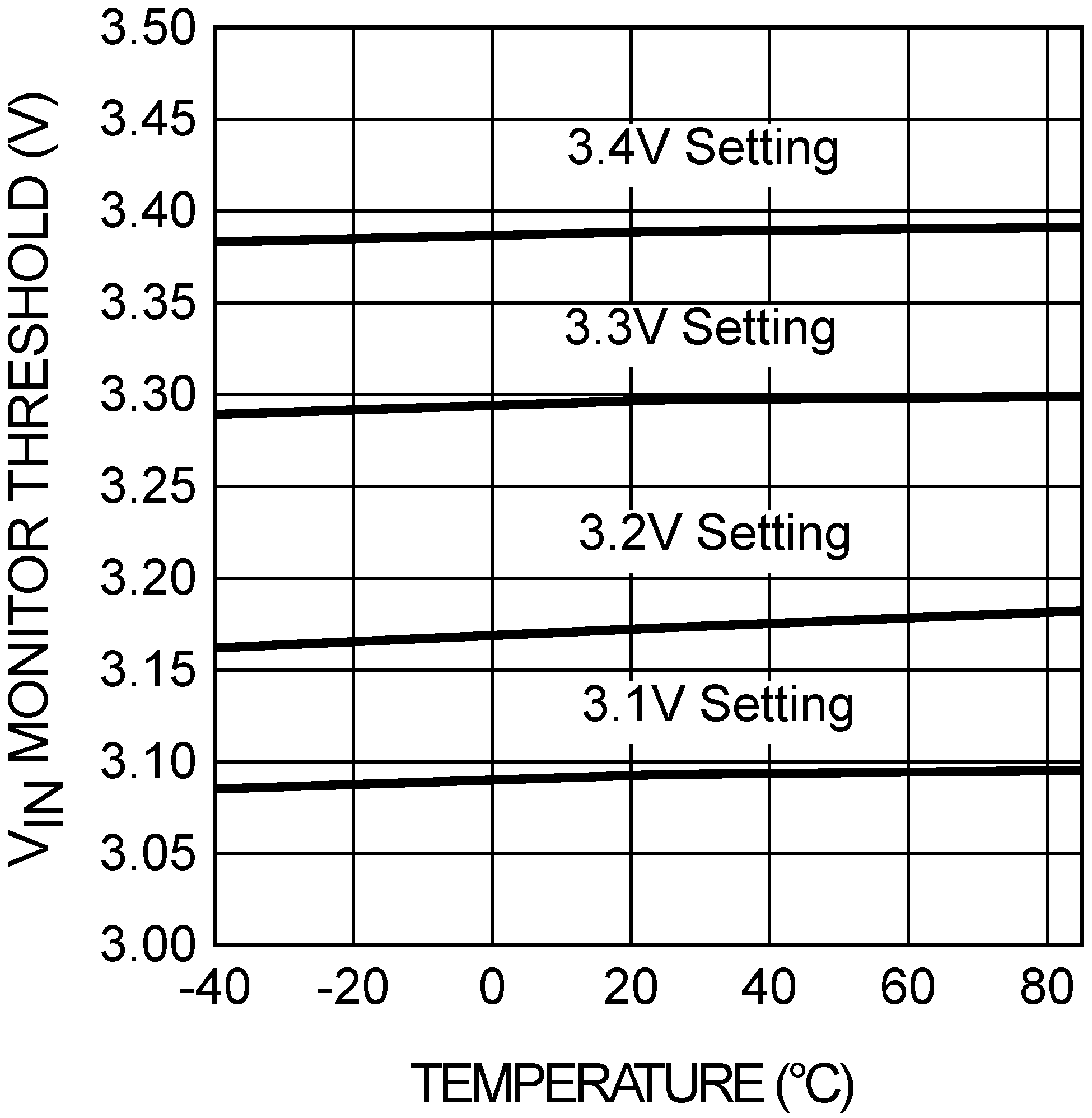
| VIN_TH | VIN monitor trip threshold | VIN falling, VIN monitor register = 0x01 (enabled with VIN_TH = 3.1 V) |
2.95 | 3.09 | 3.23 | V | |
| TX1/TORCH/GPIO1, STROBE, HWEN, ENVM/TX2/GPIO2 VOLTAGE | |||||||
| VIL | Input logic low | 2.7 V ≤ VIN ≤ 5.5 V | 0 | 0.4 | V | ||
| VIH | Input logic high | 2.7 V ≤ VIN ≤ 5.5 V | 1.2 | VIN | V | ||
| VOL | Output logic low | ILOAD = 3 mA, 2.7 V ≤ VIN ≤ 5.5 V | 400 | mV | |||
| RTX1/TORCH | Internal pulldown resistance at TX1/TORCH | 300 | kΩ | ||||
| RSTROBE | Internal pulldown resistance at STROBE | 300 | kΩ | ||||
| I2C-COMPATIBLE VOLTAGE SPECIFICATIONS (SCL, SDA) | |||||||
| VIL | Input logic low | 2.7 V ≤ VIN ≤ 5.5 V | 0 | 0.4 | V | ||
| VIH | Input logic high | 2.7 V ≤ VIN ≤ 5.5 V | 1.22 | VIN | V | ||
| VOL | Output logic low (SCL) | ILOAD = 3 mA, 2.7 V ≤ VIN ≤ 5.5 V | 400 | mV | |||
(1) All voltages are with respect to the potential at the GND pin.
(2) Minimum (MIN) and maximum (MAX) limits are ensured by design, test, or statistical analysis. Typical (TYP) numbers are not ensured, but do represent the most likely norm. Unless otherwise specified, conditions for typical specifications are: VIN = 3.6 V and TA = 25°C.
(3) The typical curve for overvoltage protection (OVP) is measured in closed loop using the Typical Application Circuit. The OVP value is found by forcing an open circuit in the LED1 and LED2 path and recording the peak value of VOUT. The value given in Electrical Characteristics is found in an open-loop configuration by ramping the voltage at OUT until the OVP comparator trips. The closed loop data can appear higher due to the stored energy in the inductor being dumped into the output capacitor after the OVP comparator trips. At worst case is an open circuit condition where the output voltage can continue to rise after the OVP comparator trips by approximately IIN× sqrt (L/COUT).
(4) The typical curve for Current Limit is measured in closed loop using the Typical Application Circuit by increasing IOUT until the peak inductor current stops increasing. The value given in Electrical Characteristics is measured open loop and is found by forcing current into SW until the current limit comparator threshold is reached. Closed loop data appears higher due to the delay between the comparator trip point and the NFET turning off. This delay allows the closed-loop inductor current to ramp higher after the trip point by approximately 20 ns × VIN / L.
5.6 Timing Requirements
See Figure 1.| MIN | NOM | MAX | UNIT | ||
|---|---|---|---|---|---|
| 1 / t1 | SCL clock frequency | 400 | kHz | ||
| t2 | Data in setup time to SCL high | 100 | ns | ||
| t3 | Data out stable after SCL low | 0 | ns | ||
| t4 | SDA low setup time to SCL low (start) | 160 | ns | ||
| t5 | SDA high hold time after SCL high (stop) | 160 | ns | ||
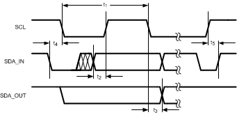 Figure 1. I2C Timing
5.7 Typical Characteristics
VIN = 3.6 V, LEDs are Lumiled PWF-4, COUT = 10 µF, CIN = 4.7 µF, L = FDSE0312-2R2 (2.2 µH, RL = 0.15 Ω), TA = 25°C, unless otherwise specified.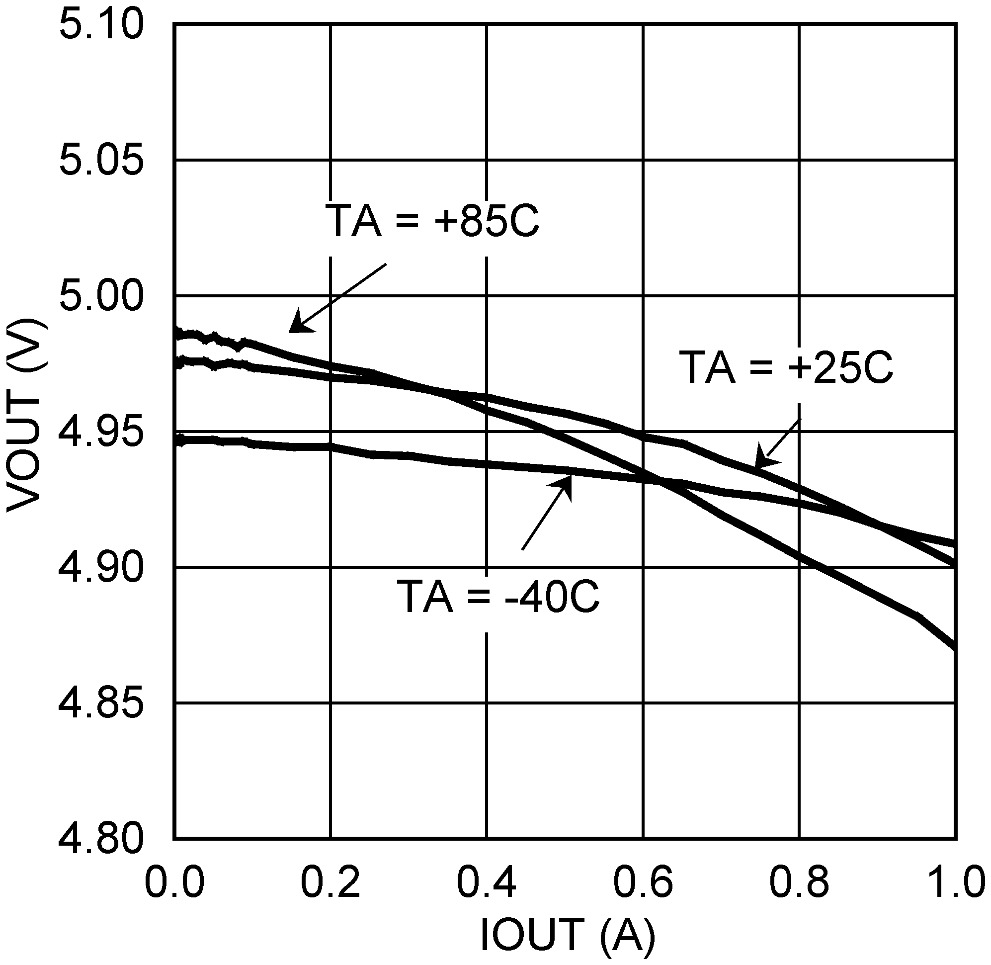
| VOUT = 5 V | Voltage-Output Mode | |
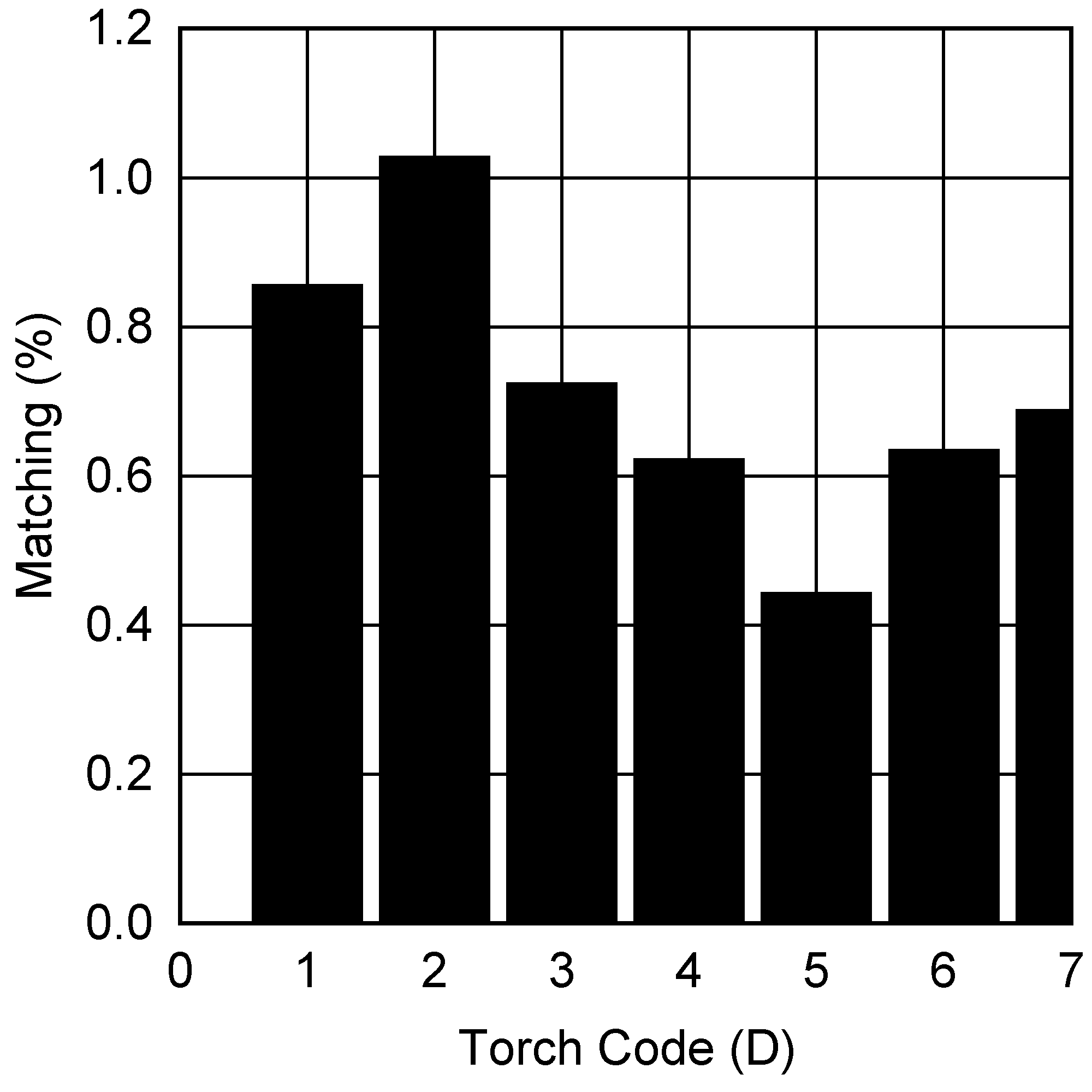
| VIN = 3.6 V | VLED1, VLED2 = 3.2 V | TA = –40°C to +85°C |
| Current Matching = Abs Value ((ILED1–ILED2)÷(ILED1+ILED2))×100 | ||
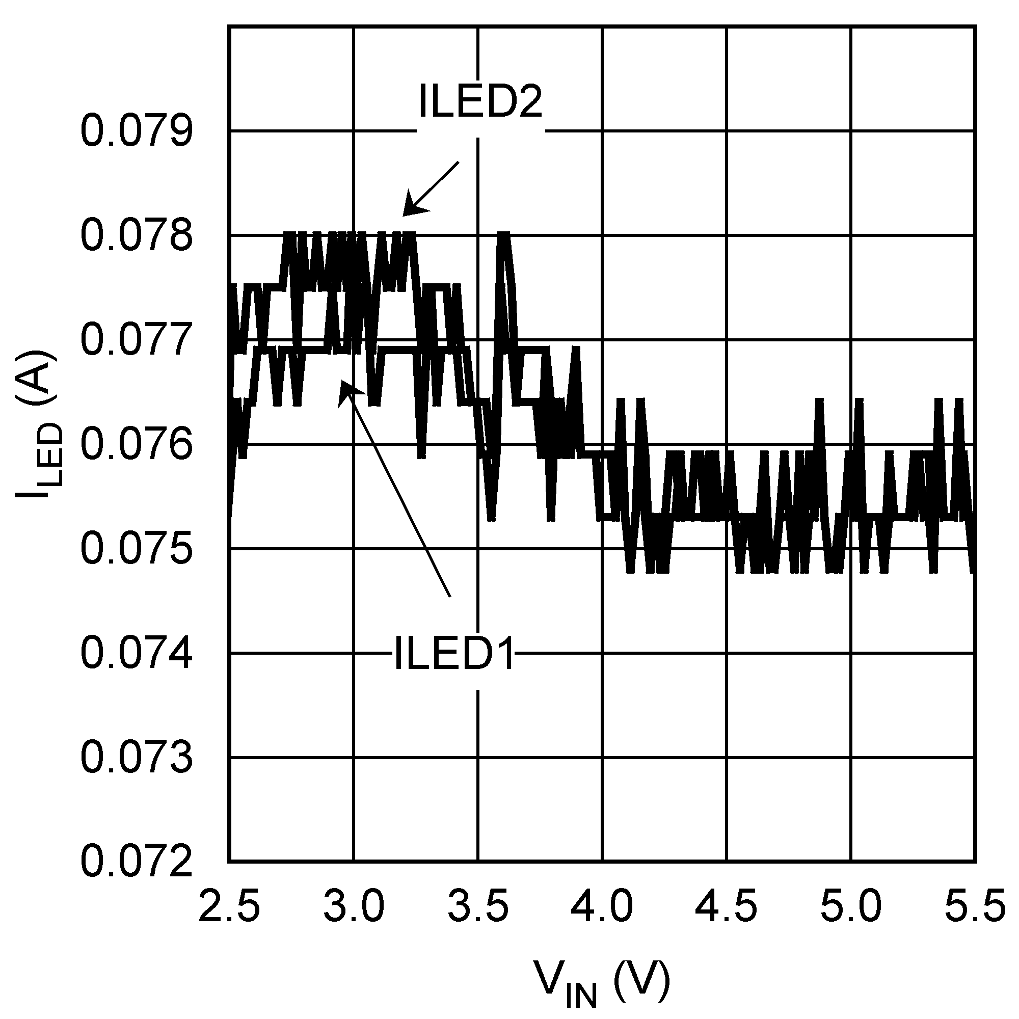
| VLED1, VLED2 = 3.2 V | 75-mA Setting | TA = 85°C |
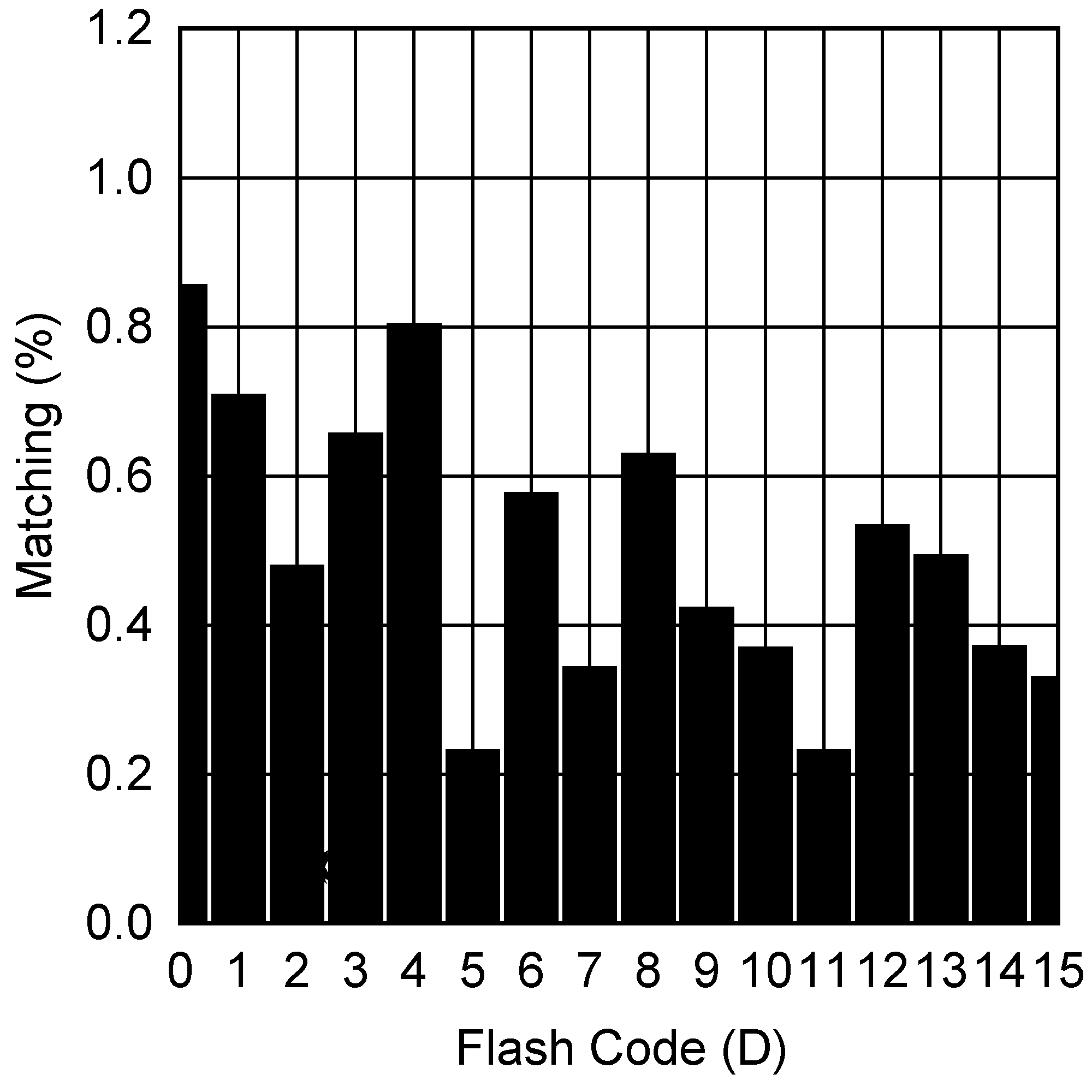
| VIN = 3.6 V | VLED1, VLED2 = 3.2 V | TA = –40°C To +85°C |
| Current Matching = Abs Value ((ILED1–ILED2)÷(ILED1+ILED2))×100 | ||
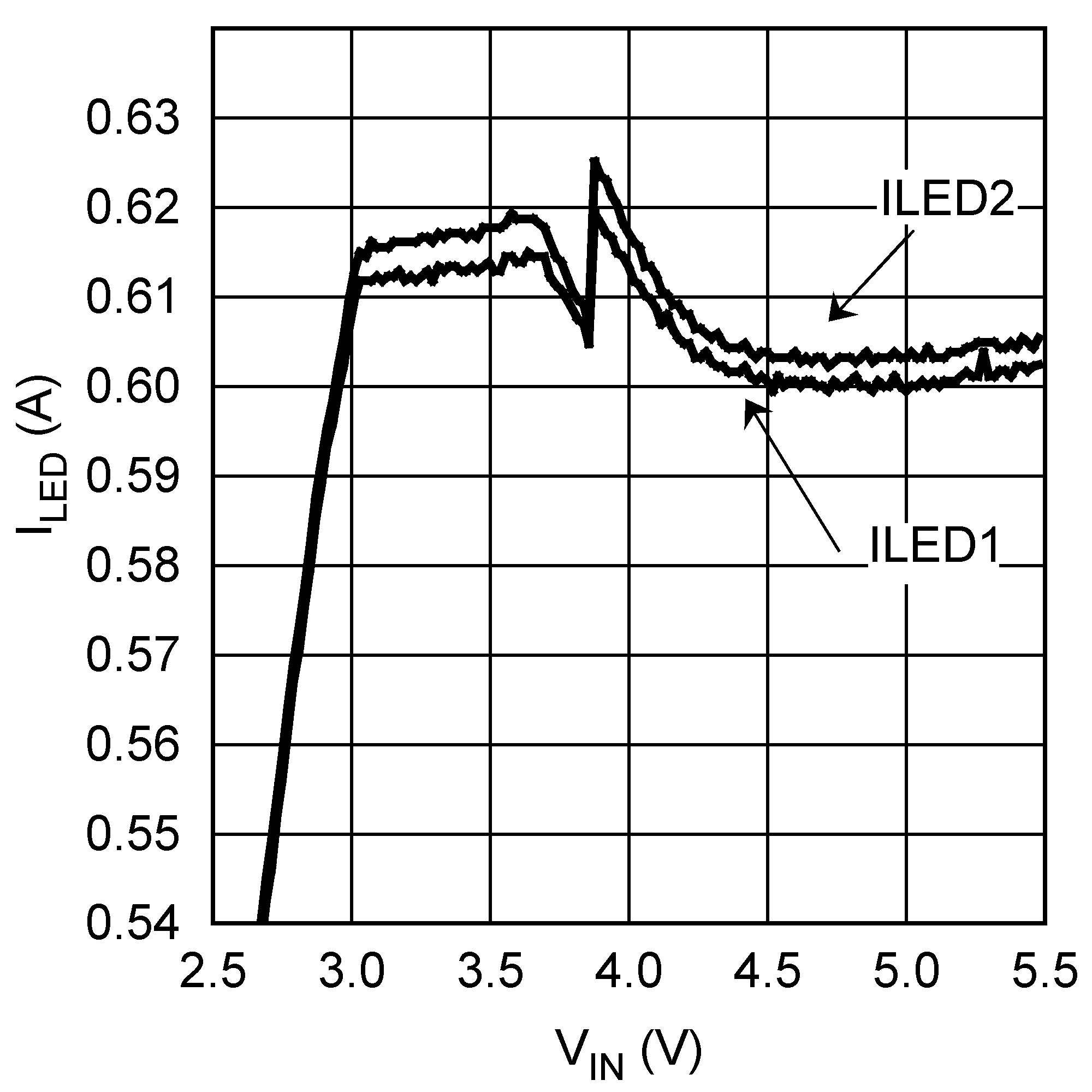
| VLED1, VLED2 = 3.2 V | 600-mA Setting | TA = 85°C |
| VLED = 1.5 V |
![LM3554 Closed Loop Current
Limit vs VIN
(Flash Duration Register Bits [6:5] = 00)) LM3554 30042085.png](/ods/images/SNVS549C/30042085.png) Figure 16. Closed Loop Current Limit vs VIN
Figure 16. Closed Loop Current Limit vs VIN
(Flash Duration Register Bits [6:5] = 00)(4))
![LM3554 Closed Loop Current
Limit vs VIN
(Flash Duration Register Bits [6:5] = 10)) LM3554 30042087.png](/ods/images/SNVS549C/30042087.png) Figure 18. Closed Loop Current Limit vs VIN
Figure 18. Closed Loop Current Limit vs VIN
(Flash Duration Register Bits [6:5] = 10)(4))
![LM3554 Indicator Current vs
VIN
(Torch Brightness Register Bits[7:6] = 01) LM3554 30042091.png](/ods/images/SNVS549C/30042091.png)
| VLEDI = 2 V |
(Torch Brightness Register Bits[7:6] = 01)
![LM3554 Indicator Current vs
VIN
(Torch Brightness Register Bits[7:6] = 11) LM3554 30042093.png](/ods/images/SNVS549C/30042093.png)
| VLEDI = 2 V |
(Torch Brightness Register Bits[7:6] = 11)
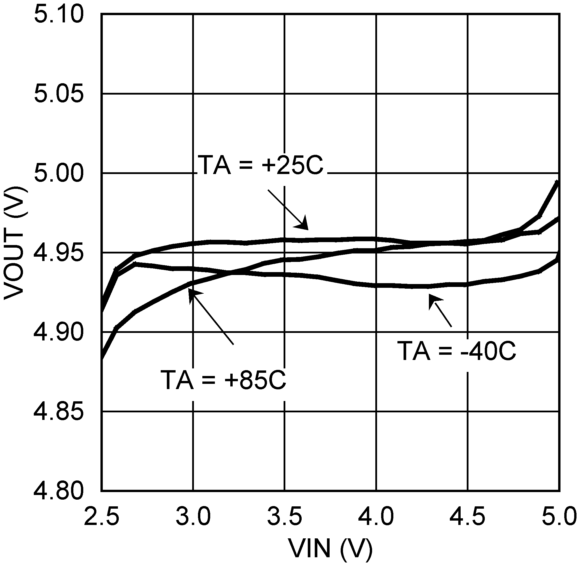
| VOUT = 5 V | Voltage-Output Mode | |
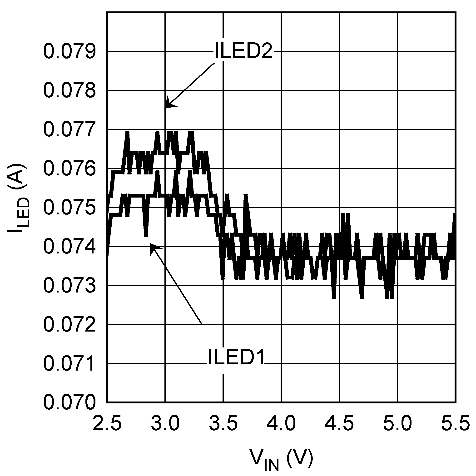
| VLED1, VLED2 = 3.2 V | 75-mA Setting | TA = 25°C |
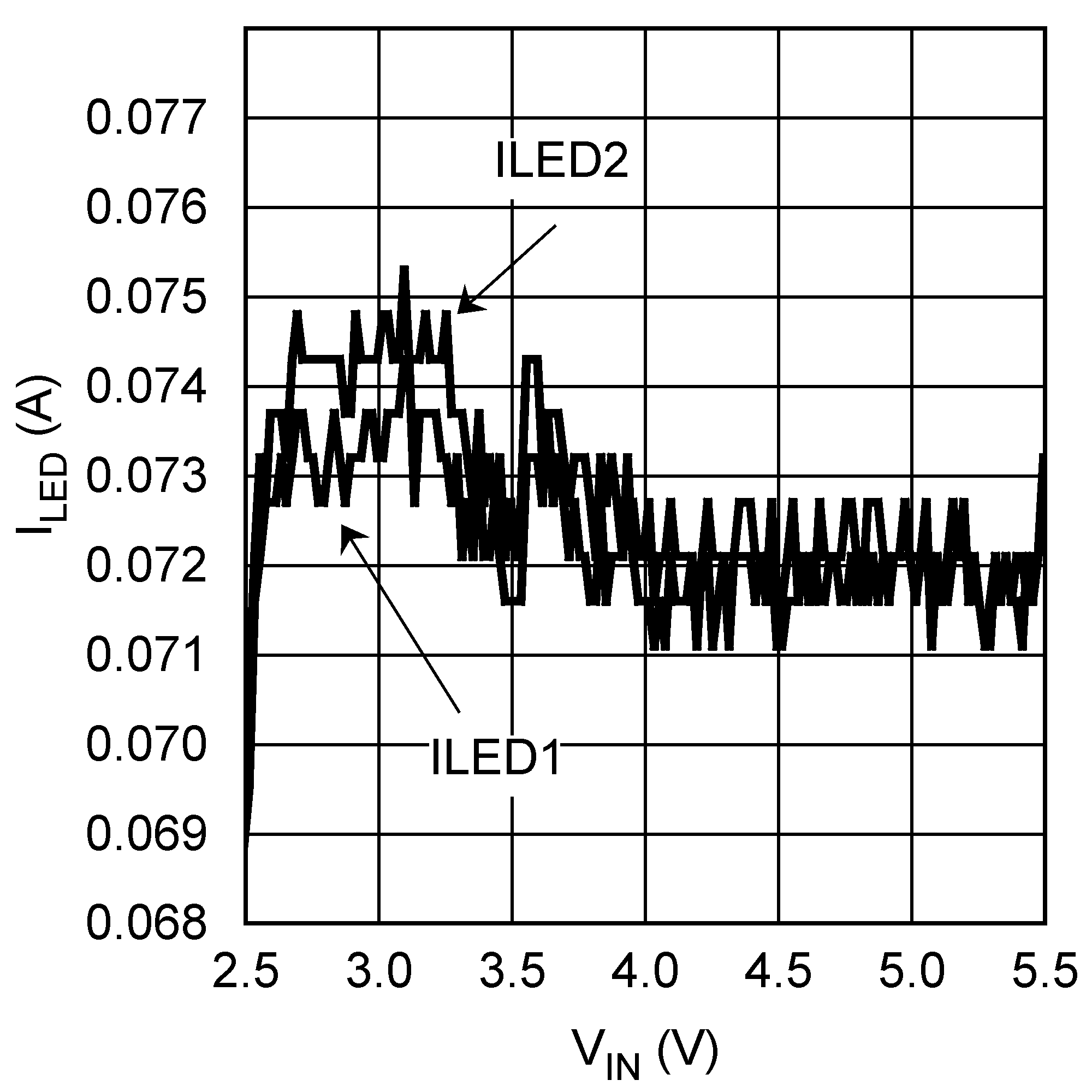
| VLED1, VLED2 = 3.2 V | 75-mA Setting | TA = –40°C |
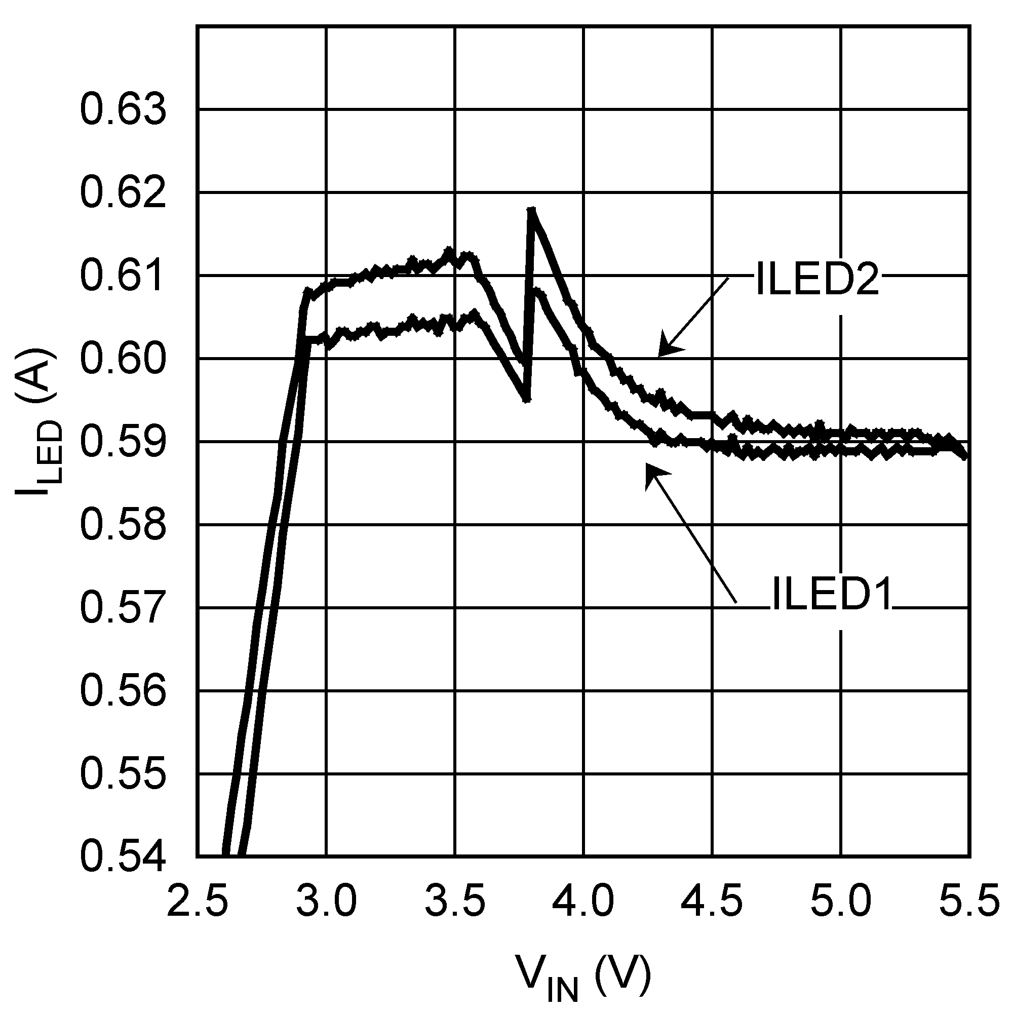
| VLED1, VLED2 = 3.2 V | 600-mA Setting | TA = 25°C |
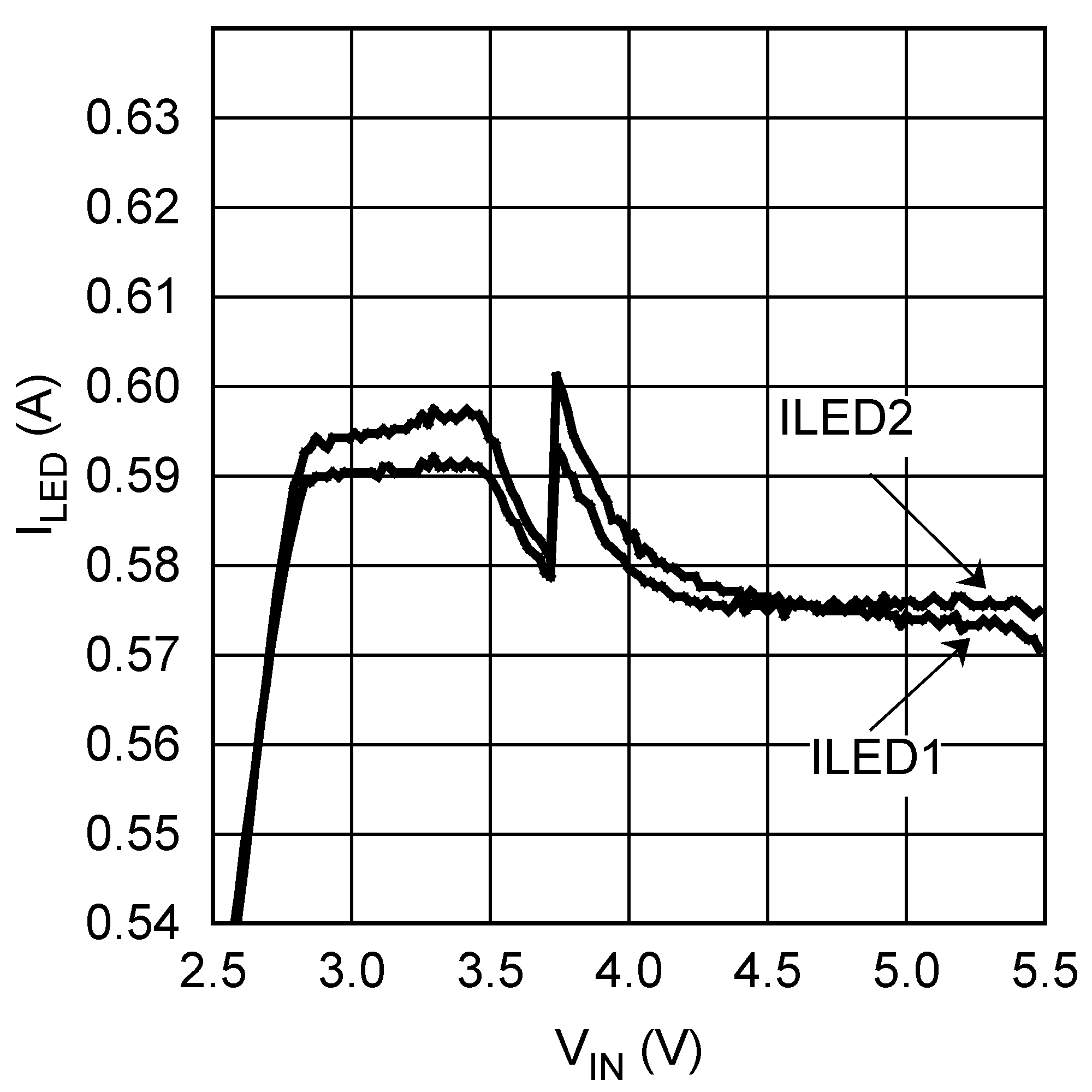
| VLED1, VLED2 = 3.2 V | 600-mA Setting | TA = –40°C |
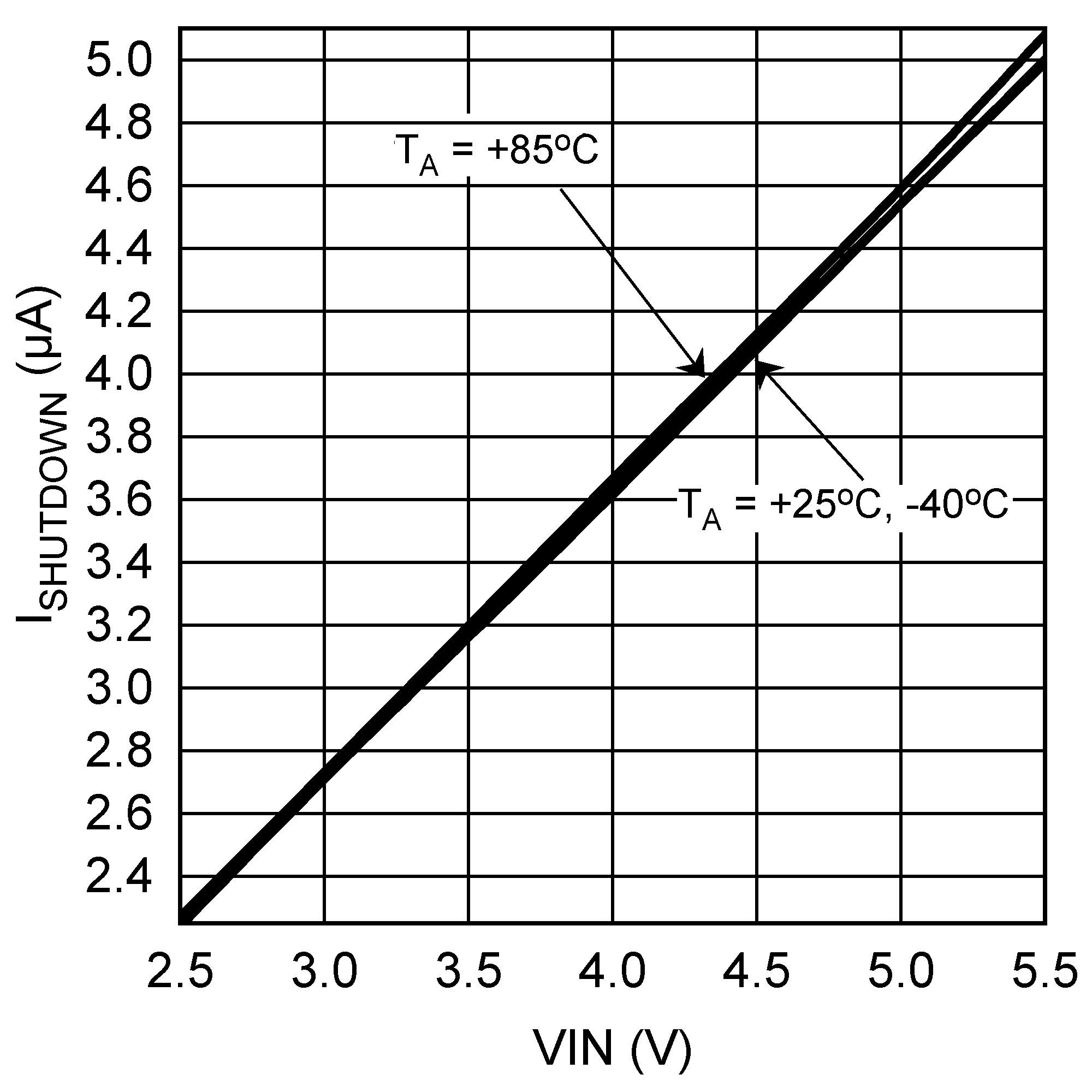
| VHWEN = 0 V |
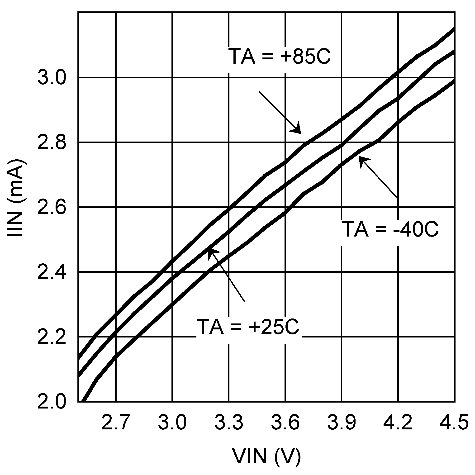
| VOUT = 5 V | IOUT = 400 mA |
![LM3554 Closed Loop Current
Limit vs VIN
(Flash Duration Register Bits [6:5] = 01) ) LM3554 30042086.png](/ods/images/SNVS549C/30042086.png) Figure 17. Closed Loop Current Limit vs VIN
Figure 17. Closed Loop Current Limit vs VIN
(Flash Duration Register Bits [6:5] = 01)(4) )
![LM3554 Closed Loop Current
Limit vs VIN
(Flash Duration Register Bits [6:5] = 11)) LM3554 30042088.png](/ods/images/SNVS549C/30042088.png) Figure 19. Closed Loop Current Limit vs VIN
Figure 19. Closed Loop Current Limit vs VIN
(Flash Duration Register Bits [6:5] = 11)(4))
![LM3554 Indicator Current vs
VIN
(Torch Brightness Register Bits[7:6] = 00) LM3554 30042090.png](/ods/images/SNVS549C/30042090.png)
| VLEDI = 2 V |
(Torch Brightness Register Bits[7:6] = 00)
![LM3554 Indicator Current vs
VIN
(Torch Brightness Register Bits[7:6] = 10) LM3554 30042092.png](/ods/images/SNVS549C/30042092.png)
| VLEDI = 2 V |
(Torch Brightness Register Bits[7:6] = 10)
