SNVS549C June 2009 – February 2016 LM3554
PRODUCTION DATA.
- 1 Features
- 2 Applications
- 3 Description
- 4 Revision History
- 5 Specifications
-
6 Detailed Description
- 6.1 Overview
- 6.2 Functional Block Diagram
- 6.3
Feature Description
- 6.3.1 Start-Up
- 6.3.2 Overvoltage Protection
- 6.3.3 Current Limit
- 6.3.4 Flash Termination (Strobe-Initiated Flash)
- 6.3.5 Flash Termination (I2C-Initiated Flash)
- 6.3.6 Flash Timeout
- 6.3.7 Torch Mode
- 6.3.8 TX1/Torch
- 6.3.9 ENVM/TX2/GPIO2
- 6.3.10 Indicator LED/Thermistor (LEDI/NTC)
- 6.3.11 Alternative External Torch (AET Mode)
- 6.3.12 Input Voltage Monitor
- 6.3.13 LM3554 Timing Diagrams
- 6.3.14 Flags Register and Fault Indicators
- 6.3.15 Thermal Shutdown
- 6.3.16 LED Fault
- 6.3.17 Flash Timeout
- 6.3.18 LED Thermal Fault
- 6.3.19 Input Voltage Monitor Fault
- 6.3.20 TX1 And TX2 Interrupt Flags
- 6.3.21 Light Load Disable
- 6.4 Device Functional Modes
- 6.5 Programming
- 6.6 Register Maps
-
7 Application and Implementation
- 7.1 Application Information
- 7.2
Typical Application
- 7.2.1 Design Requirements
- 7.2.2 Detailed Design Procedure
- 7.2.3 Application Curves
- 8 Power Supply Recommendations
- 9 Layout
- 10Device and Documentation Support
- 11Mechanical, Packaging, and Orderable Information
Package Options
Mechanical Data (Package|Pins)
- YFQ|16
Thermal pad, mechanical data (Package|Pins)
Orderable Information
6 Detailed Description
6.1 Overview
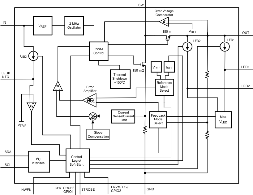
The LM3554 is a high-power white-LED flash driver capable of delivering up to 1.2-A of LED current into a single LED, or up to 600 mA into two parallel LEDs. The device incorporates a 2-MHz constant frequency, synchronous, current mode PWM boost converter, and two high-side current sources to regulate the LED current over the 2.5-V to 5.5-V input voltage range.
The LM3554 operates in two modes: LED mode or constant voltage-output mode. In LED mode when the output voltage is greater than VIN – 150 mV, the PWM converter switches and maintains at least 300 mV (VHR) across both current sources (LED1 and LED2). This minimum headroom voltage ensures that the current sinks remain in regulation. When the input voltage is above VLED + VHR, the device operates in pass mode with the device not switching and the PFET on continuously. In pass mode the difference between (VIN – ILED × RON_P) and VLED is dropped across the current sources. If the device is operating in pass mode, and VIN drops to a point that forces the device into switching, the device goes into switching mode one time. The LM3554 remains in switching mode until the device is shut down and re-enabled. This is true even if VIN rises back above VLED + 300 mV during the current flash or torch cycle. This prevents the LED current from oscillating when VIN is operating close to VOUT.
In voltage-output mode the LM3554 operates as a voltage output boost converter with selectable output voltages of 4.5 V and 5 V. In this mode the LM3554 is able to deliver up to typically 5 W of output power. At light loads and in voltage-output mode the PWM switching converter changes over to a pulsed frequency regulation mode and only switches as necessary to ensure proper LED current or output voltage regulation. This allows for improved light load efficiency compared to converters that operate in fixed-frequency PWM mode at all load currents.
Additional features of the LM3554 include four logic inputs, an internal comparator for LED thermal sensing, and a low-power indicator LED current source. The STROBE input provides a hardware flash mode enable. The ENVM/TX2/GPIO2 input is configurable as a hardware voltage-output mode enable (ENVM), an active high flash interrupt that forces the device from flash mode to a low-power TORCH mode (TX2), or as a programmable logic input/output (GPIO2). The TX1 input is configurable as an active high flash interrupt that forces the device from flash mode to a low-power torch mode (TX1), as a hardware torch mode enable (TORCH), or as a programmable logic input/output (GPIO1) . The HWEN input provides for an active low hardware shutdown of the device. Finally, the LEDI/NTC pin is configurable as a low-power indicator LED driver (LEDI), or as a threshold detector for thermal sensing (NTC). In NTC mode when the threshold (VTRIP) at the LEDI/NTC pin is crossed (VLEDI/NTC falling), the flash pulse is forced to the torch current setting, or into shutdown depending on the NTC shutdown bit setting.
The device is controlled via an I2C-compatible interface. This includes switchover from LED to voltage-output mode, adjustment of the LED current in torch mode, adjustment of the LED current in flash mode, adjustment of the indicator LED currents, changing the flash LED current duration, changing the switch current limit. Additionally, there are 5 flag bits that can be read back indicating flash current timeout, overtemperature condition, LED failure (open or short), LED thermal failure, and an input voltage fault.
6.2 Functional Block Diagram
6.3 Feature Description
6.3.1 Start-Up
The device is turned on through bits [2:0] of the Torch Brightness Register (0xA0), bits [2:0] of the Flash Brightness Register (0xB0), the ENVM input, or the STROBE input. Bits [1:0] of the Torch Brightness Register or Flash Brightness Register enables/disables the current sources (LED1, LED2, and LEDI). Bit [2] enables/disables the voltage-output mode. A logic high at STROBE enables flash mode. A logic high on the ENVM input forces the LM3554 into voltage-output mode.
On start-up, when VOUT is less than VIN the internal synchronous PFET turns on as a current source and delivers typically 350 mA to the output capacitor. During this time all current sources (LED1, LED2, and LEDI) are off. When the voltage across the output capacitor reaches 2.2 V, the current sources can turn on. At turnon the current sources step through each flash or torch level until the target LED current is reached (16 µs/step). This gives the device a controlled turnon and limits inrush current from the VIN supply.
6.3.2 Overvoltage Protection
The output voltage is limited to typically 5.6 V (5.7 V maximum). In situations such as the current source open, the LM3554 raises the output voltage in order to keep the LED current at its target value. When VOUT reaches 5.6 V the overvoltage comparator trips and turns off both the internal NFET and PFET. When VOUT falls below 5.4 V (typical), the LM3554 begins switching again.
6.3.3 Current Limit
The LM3554 features four selectable current limits: 1 A, 1.5 A, 2 A, and 2.5 A. These are selectable through the I2C-compatible interface via bits 5 (CL0) and 6 (CL1) of the Flash Duration Register. When the current limit is reached, the LM3554 device stops switching for the remainder of the switching cycle.
Because the current limit is sensed in the NMOS switch there is no mechanism to limit the current when the device operates in pass mode. In situations where there could potentially be large load currents at OUT, and the LM3554 is operating in Pass mode, the load current must be limited to 2.5 A. In boost mode or pass mode if VOUT falls below approximately 2.3 V, the device stops switching, and the PFET operates as a current source limiting the current to typically 350 mA. This prevents damage to the LM3554 and excessive current draw from the battery during output short circuit conditions.
6.3.4 Flash Termination (Strobe-Initiated Flash)
Bit [7] of the Flash Brightness Register (STR bit) determines how the flash pulse terminates with STROBE-initated flash pulses. With the STR bit = 1 the Flash current pulseonly terminates by reaching the end of the flash-timeout period. With STR = 0, Flash mode can be terminated by pulling STROBE low, or by allowing the flash-timeout period to elapse. If STR = 0 and STROBE is toggled before the end of the flash-timeout period, the timeout period resets on the rising edge of STROBE. See LM3554 Timing Diagrams regarding the flash pulse termination for the different STR bit settings.
After the flash pulse terminates, either by a flash timeout, or pulling STROBE low, LED1 and LED2 turn completely off. This happens even when Torch is enabled via the I2C-compatible interface, and the flash pulse is turned on by toggling STROBE. After a flash event ends the EN1, EN0 bits (bits [1:0] of the Torch Brightness Register, or Flash Brightness Register) are automatically re-written with (0, 0).
6.3.5 Flash Termination (I2C-Initiated Flash)
For I2C-initiated flash pulses, the flash LED current can be terminated by either waiting for the timeout duration to expire or by writing a (0, 0) to bits [1:0] of the Torch Brightness Register, or Flash Brightness Register. If the timeout duration is allowed to elapse, the flash enable bits of the Torch Brightness and Flash Brightness Registers are automatically reset to 0.
6.3.6 Flash Timeout
The flash timeout period sets the duration of the flash current pulse. Bits [4:0] of the Flash Duration Register programs the 32 different flash timeout levels in steps of 32 ms giving a flash timeout range of 32 ms to 1024 ms (see Table 4).
6.3.7 Torch Mode
In torch mode the current sources LED1 and LED2 each provide 8 different current levels (see Table 2). The torch currents are adjusted by writing to bits [5:3] of the Torch Brightness Register. Torch mode is activated by setting Torch Brightness Register bits [1:0] to (1, 0) or Flash Brightness bits [1:0] to (1, 0). Once the torch mode is enabled the current sources ramp up to the programmed torch current level by stepping through all of the torch currents at 16 µs/step until the programmed torch current level is reached.
6.3.8 TX1/Torch
The TX1/TORCH/GPIO1 input has a triple function. With Configuration Register 1 Bit [7] = 0 (default), TX1/TORCH/GPIO1 is a power amplifier synchronization input (TX1 mode). This is designed to reduce the current pulled from the battery during an RF power amplifier transmit event. When the LM3554 is engaged in a flash event, and the TX1 pin is pulled high, both LED1 and LED2 are forced into torch mode at the programmed torch current setting. If the TX1 pin is then pulled low before the flash pulse terminates the LED current ramps back to the previous flash current level. At the end of the flash timeout whether the TX1 pin is high or low, the LED current turns off.
With the Configuration Register Bit [7] = 1, TX1/TORCH/GPIO1 is configured as a hardware torch mode enable (TORCH). In this mode a high at TORCH turns on the LED current sources in torch mode. STROBE (or I2-initiated flash) takes precedence over the TORCH mode input. Figure 37 details the functionality of the hardware TORCH mode. Additionally, when a flash pulse is initiated during hardware TORCH mode, the hardware torch mode bit is reset at the end of the flash pulse. In order to re-enter hardware torch mode, bit [7] of Configuration Register 1 would have to be re-written with a 1.
The TX1/TORCH/GPIO1 input can also be configured as a GPIO input/output. for details on this, refer to the GPIO Register section of the datasheet.
6.3.9 ENVM/TX2/GPIO2
The ENVM/TX2/GPIO2/INT pin has four functions. In ENVM mode (Configuration Register 1 bit [5] = 0), the ENVM/TX2/GPIO2/INT pin is an active high logic input that forces the LM3554 into voltage-output mode. In TX2 mode (Configuration Register 1 bit [5] = 1), the ENVM/TX2/GPIO2/INT pin is a Power Amplifier Synchronization input that forces the LM3554 from Flash mode into Torch mode. In GPIO2 mode (GPIO Register Bit [3] = 1) the ENVM/TX2/GPIO2/INT pin is configured as a general purpose logic input/output and controlled via bits[3:5] of the GPIO Register. In INT mode the ENVM/TX2/GPIO2/INT pin is a hardware interrupt output which pulls low when the LM3554 is in NTC mode, and the voltage at LEDI/NTC falls below VTRIP.
In TX2 mode, when Configuration Register 1 bit [6] = 0 the ENVM/TX2/GPIO2 pin is an active low transmit interrupt input. Under this condition, when the LM3554 is engaged in a flash event, and ENVM/TX2/GPIO2 is pulled low, both LED1 and LED2 are forced into either torch mode or LED shutdown depending on the logic state of Configuration Register 2 bit [0]. In TX2 mode with Configuration Register 1 bit [6] = 1, the ENVM/TX2/GPIO2 pin is an active high transmit interrupt. Under this condition when the LM3554 is engaged in a Flash event, and the TX2 pin is driven high, both LED1 and LED2 are forced into torch mode or LED shutdown, depending on the logic state of Configuration Register 2 bit [0]. After a TX2 event, if the ENVM/TX2/GPIO2 pin is disengaged, and the TX2 Shutdown bit is set to force Torch mode, the LED current ramps back to the previous Flash current level. If the TX2 shutdown bit is programmed to force LED shutdown upon a TX2 event the Flags Register must be read to resume normal LED operation. Table 5, Figure 33, and Figure 34 detail the Functionality of the ENVM/TX2 input.
6.3.9.1 ENVM/TX2/GPIO2/INT as an Interrupt Output
In GPIO2 mode the ENVM/TX2/GPIO2 pin can be made to reflect the inverse of the LED Thermal Fault flag (bit[5] in the Flags Register). To configure the LM3554 for this feature:
set GPIO Register Bit [6] = 1 (NTC External Flag)
set GPIO Register Bit [3] = 1 (GPIO2 mode)
set GPIO Register Bit [4] = 1 (GPIO2 is an output)
set Configuration Register 1 Bit [3] = 1 (NTC mode)
When the voltage at the LEDI/NTC pin falls below VTRIP (1.05 V typical), the LED Thermal Fault Flag (bit [5] in the Flags Register) is set, and the ENVM/TX2/GPIO2/INT pin is forced low. In this mode the interrupt can only be reset to the open-drain state by reading back the Flags register.
6.3.10 Indicator LED/Thermistor (LEDI/NTC)
The LEDI/NTC pin serves a dual function: either as an LED indicator driver or as a threshold detector for a negative temperature coefficient (NTC) thermistor.
6.3.10.1 LED Indicator Mode (LEDI)
LEDI/NTC is configured as an LED indicator driver by setting Configuration Register 1 bit [3] = (0) and Torch Brightness Register bits [1:0] = (0, 1), or Flash Brightness Register bits [1:0] = (0, 1). In Indicator mode there are 4 different current levels available (2.3 mA, 4.6 mA, 6.9 mA, 8.2 mA). Bits [7:6] of the Torch Brightness Register set the 4 different indicator current levels. The LEDI current source has a 1-V typical headroom voltage.
6.3.10.2 Thermal Comparator Mode (NTC)
Writing a 1 to Configuration Register 1 bit [3] disables the indicator current source and configures the LEDI/NTC pin as a detector for an NTC thermistor. In this mode LEDI/NTC becomes the negative input of an internal comparator with the positive input internally connected to a reference (VTRIP = 1.05 V typical). Additionally, Configuration Register 2 bit [1] determines the action the device takes if the voltage at LEDI/NTC falls below VTRIP (while the device is in NTC mode). With the Configuration Register 2 bit [1] = 0, the LM3554 is forced into torch mode when the voltage at LEDI/NTC falls below VTRIP. With the Configuration Register 2 bit [1] = 1 the device shuts down the current sources when VLEDI/NTC falls below VTRIP. When the LM3554 is forced from flash into torch (by VLEDI/NTC falling below VTRIP), normal LED operation (during the same flash pulse) can only be re-started by reading from the Flags Register (0xD0) and ensuring the voltage at VLEDI/NTC is above VTRIP. When VLEDI/NTC falls below VTRIP, and the Flags register is cleared, the LM3554 goes through a 250-µs deglitch time before the flash current falls to either torch mode or goes into shutdown.
6.3.11 Alternative External Torch (AET Mode)
Configuration Register 2 bit [2] programs the LM3554 for AET mode. With this bit set to 0 (default) TX1/TORCH is a transmit interrupt that forces torch mode only during a flash event. For example, if TX1/TORCH goes high during a flash event then the LEDs is forced into torch mode only for the duration of the timeout counter. At the end of the timeout counter the LEDs turn off.
With Configuration Register 2 bit [2] set to (1) the operation of TX1/TORCH becomes dependent on its occurrence relative to STROBE. In this mode if TX1/TORCH goes high first, then STROBE goes high, the LEDs are forced into torch mode with no timeout. In this mode if TX1/TORCH goes high after STROBE has gone high then the TX1/TORCH pin operates as a normal TX interrupt, and the LEDs turn off at the end of the timeout duration. (See LM3554 Timing Diagrams, Figure 35, and Figure 36.)
6.3.12 Input Voltage Monitor
The LM3554 has an internal comparator that monitors the voltage at IN, which can force the LED current into torch mode or into shutdown if VIN falls below the programmable VIN monitor threshold. Bit 0 in the VIN Monitor Register (0x80) enables or disables this feature. When enabled, bits 1 and 2 program the four adjustable thresholds of 3.1 V, 3.2 V, 3.3 V, and 3.4 V. Bit 3 in Configuration Register 2 (0xF0) selects whether an undervoltage event forces torch mode or forces the LEDs off. See /Table 7 and /Table 9 for additional information.
There is a set 100-mV hysteresis for the input voltage monitor. When the input voltage monitor is active, and VIN falls below the programmed VIN monitor threshold, the LEDs either turn off or their current is reduced to the programmed torch current setting. To reset the LED current to its previous level, two things must occur. First, VIN must go at least 100 mV above the UVLO threshold and secondly, the Flags Register must be read back.
6.3.13 LM3554 Timing Diagrams
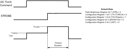 Figure 28. Normal Torch-to-Flash Operation (Default, Power On or LM3554 Reset State)
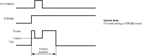 Figure 29. TX1 Event During A Flash Event
(Default State,TX1/Torch is an Active High TX Input)
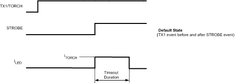 Figure 30. TX1 Event Before and After Flash Event
(Default State, TX1/Torch is an Active High TX Input)
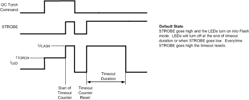 Figure 31. Strobe Input is Level Sensitive (Default State, STR Bit = 0)
 Figure 32. Strobe Input is Edge Sensitive (STR Bit = 1)
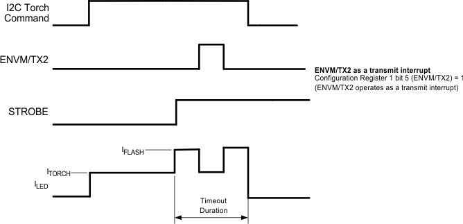 Figure 33. ENVM/TX2 Pin is Configured as an Active High TX Input
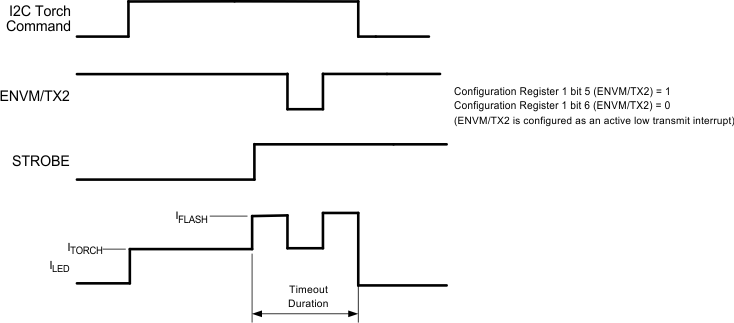 Figure 34. ENVM/TX2 Pin is Configured as an Active Low TX Input
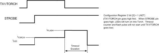 Figure 35. Alternative External Torch Mode (TX1/Torch Turns on Before Strobe)
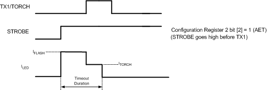 Figure 36. Alternative External Torch Mode
(Strobe Goes High Before TX1/Torch, Same As Default With SEM = 0)
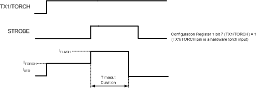 Figure 37. TX1/Torch Configured as a Hardware Torch Input
6.3.14 Flags Register and Fault Indicators
The Flags Register (0xD0) contains the Interrupt and fault indicators. Five fault flags are available in the LM3554. These include a thermal shutdown, an LED failure flag (LEDF) , a Timeout indicator Flag (TO), a LED Thermal Flag (NTC), and a VIN Monitor Flag. Additionally, two interrupt flag bits TX1 interrupt and TX2 interrupt indicate a change of state of the TX1/TORCH pin (TX1 mode) and ENVM/TX2 pin (TX2 mode). Reading back a 1 indicates the TX lines have changed state since the last read of the Flags Register. A read of the Flags Register resets these bits.
6.3.15 Thermal Shutdown
When the device die temperature reaches 150°C the boost converter shuts down, and the NFET and PFET turn off. Additionally, all three current sources (LED1, LED2, and LEDI) turn off. When the thermal shutdown threshold is tripped a 1 is written to bit [1] of the Flag Register (Thermal Shutdown bit). The LM3554 starts up again when the die temperature falls to below 135°C.
During heavy load conditions when the internal power dissipation in the device causes thermal shutdown, the device turns off and starts up again after the die temperature cools, resulting in a pulsed on/off operation. The OVT bit, however, is only written once. To reset the OVT bit pull HWEN low, power down the LM3554, or read the Flags Register.
6.3.16 LED Fault
The LED Fault flag (bit 2 of the Flags Register) reads back a 1 if the part is active in flash or torch mode and either LED1 or LED2 experience an open or short condition. An LED open condition is signaled if the OVP threshold is crossed at OUT while the device is in flash or torch mode. An LED short condition is signaled if the voltage at LED1 or LED2 goes below 500 mV while the device is in torch or flash mode.
There is a delay of 250 µs before the LEDF flag is valid on a LED short. This is the time from when VLED falls below the LED short threshold of 500 mV (typical) to when the fault flag is valid. There is a delay of 2 µs from when the LEDF flag is valid on an LED open. This delay is the time between when the OVP threshold is triggered and when the fault flag is valid. The LEDF flag can only be reset to 0 by pulling HWEN low, removing power to the LM3554, or reading the Flags Register.
6.3.17 Flash Timeout
The TO flag (bit [0] of the Flags Register) reads back a 1 if the LM3554 is active in flash mode and the timeout period expires before the flash pulse is terminated. The flash pulse can be terminated before the timeout period expires by pulling the STROBE pin low (with STR bit 0), or by writing a 0 to bit 0 or 1 of the Torch Brightness Register or the Flash Brightness Register. The TO flag is reset to 0 by pulling HWEN low, removing power to the LM3554 device, reading the Flags Register, or when the next flash pulse is triggered.
6.3.18 LED Thermal Fault
The NTC flag (bit [5] of the Flags Register) reads back a 1 if the LM3554 is active in flash or torch mode, the device is in NTC mode, and the voltage at LEDI/NTC has fallen below VTRIP (1.05 V typical). When this has happened and the LM3554 has been forced into torch or LED shutdown (depending on the state of Configuration Register 2 bit [1], the Flags Register must be read in order to place the device back in normal operation. (See Thermal Comparator Mode (NTC) for more details.)
6.3.19 Input Voltage Monitor Fault
The VIN Monitor Flag (bit [6] of the Flag Register) reads back a 1 when the Input Voltage Monitor is enabled and VIN falls below the programmed VIN Monitor threshold. This flag must be read back in order to resume normal operation after the LED current has been forced to Torch mode or turned off due to a VIN Monitor event.
6.3.20 TX1 And TX2 Interrupt Flags
The TX1 and TX2 interrupt flags (bits [3] and [4]) indicate a TX event on the TX1/TORCH and ENVM/TX2 pins. Bit 3 is read back a 1 if TX1/TORCH is in TX1 mode and the pin has changed from low to high since the last read of the Flags Register. Bit 4 reads back a 1 if ENVM/TX2 is in TX2 mode and the pin has had a TX event since the last read of the Flags Register. A read of the Flags Register automatically resets these bits.
The ENVM/TX2/GPIO2 pin, when configured in TX2 mode, has a TX event that can be either a high-to-low transition or a low-to-high transition depending on the setting of the TX2 polarity bit (see Table 6).
6.3.21 Light Load Disable
Configuration Register 1 bit [0] = 1 disables the light load comparator. With this bit set to 0 (default) the light load comparator is enabled. Light load mode only applies when the LM3554 is active in voltage-output mode. In LED mode the light load comparator is always disabled. When the light load comparator is disabled the LM3554 operates at a constant frequency down to ILOAD = 0. Disabling light load can be useful when a more predictable switching frequency across the entire load current range is desired.
6.4 Device Functional Modes
6.4.1 Flash Mode
In flash mode the LED current sources (LED1 and LED2) each provide 16 different current levels from typically 34 mA to approximately 600 mA. The flash currents are set by writing to bits [6:3] of the Flash Brightness Resister. Flash mode is activated by either writing a (1, 1) to bits [1:0] of the Torch Brightness Register, writing a (1, 1) to bit [1:0] of the Flash Brightness Register, or by pulling the STROBE pin high. Once the Flash sequence is activated, both current sinks (LED1 and LED2) ramps up to the programmed Flash current by stepping through all Flash levels (16 µs/step) until the programmed current is reached.
6.4.2 Pass Mode
Once the output voltage charges up to VIN – 150 mV the the device operates either in pass mode or boost mode. If the voltage difference between VOUT and VLED is less than 300 mV, the device transitions in boost mode. If the difference between VOUT and VLED is greater than 300 mV, the device operates in pass mode. In pass mode the boost converter stops switching, and the synchronous PFET turns fully on bringing VOUT up to VIN – IIN × RPMOS (RPMOS = 150 mΩ). In pass mode the inductor current is not limited by the peak current limit. In this situation the output current must be limited to 2.5A.
6.4.3 Voltage-Output Mode
Bit 2 (VM) of the Torch Brightness Register, bit 2 (VM) of the Flash Brightness Register, or the ENVM input enables or disables the voltage-output mode. In voltage-output mode the device operates as a simple boost converter with two selectable voltage levels (4.5 V and 5 V). Write a 1 to bit 1 (OV) of Configuration Register 1 to set VOUT to 5 V. Write a 0 to this bit to set VOUT to 4.5 V. In voltage-output mode the LED current sources can continue to operate; however, the difference between VOUT and VLED is dropped across the current sources. (See Maximum Output Power.) In voltage-output mode when VIN is greater than VOUT the LM3554 device operates in pass mode (see Pass Mode).
At light loads the LM3554 switches over to a pulsed frequency mode operation (light load comparator enabled). In this mode the device only switches as necessary to maintain VOUT within regulation. This mode provides a better efficiency due to the reduction in switching losses which become a larger portion of the total power loss at light loads.
6.5 Programming
6.5.1 I2C-Compatible Interface
6.5.1.1 Start and Stop Conditions
The LM3554 is controlled via an I2C-compatible interface. START and STOP conditions classify the beginning and end of the I2C session. A START condition is defined as SDA transitioning from HIGH to LOW while SCL is HIGH. A STOP condition is defined as SDA transitioning from LOW to HIGH while SCL is HIGH. The I2C master always generates the START and STOP conditions.
 Figure 38. Start and Stop Sequences
The I2C bus is considered busy after a START condition and free after a STOP condition. During data transmission the I2C master can generate repeated START conditions. A START and a repeated START condition are equivalent function-wise. The data on SDA must be stable during the HIGH period of the clock signal (SCL). In other words, the state of SDA can only be changed when SCL is LOW. Figure 1 and Figure 39 show the SDA and SCL signal timing for the I2C-Compatible Bus. See Electrical Characteristics for timing values.
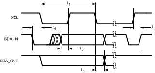 Figure 39. I2C-Compatible Timing
6.5.1.2 I2C-Compatible Chip Address
The device address for the LM3554 is 1010011 (53). After the START condition, the I2C master sends the 7-bit address followed by an eighth bit, read or write (R/W). R/W = 0 indicates a WRITE and R/W = 1 indicates a READ. The second byte following the device address selects the register address to which the data will be written. The third byte contains the data for the selected register.
 Figure 40. Device Address
6.5.1.3 Transferring Data
Every byte on the SDA line must be eight bits long, with the most significant bit (MSB) transferred first. Each byte of data must be followed by an acknowledge bit (ACK). The acknowledge related clock pulse (9th clock pulse) is generated by the master. The master releases SDA (HIGH) during the 9th clock pulse (write mode). The LM3554 pulls down SDA during the 9th clock pulse, signifying an acknowledge. An acknowledge is generated after each byte has been received.
6.6 Register Maps
6.6.1 Register Descriptions
Table 1. LM3554 Internal Registers
| REGISTER NAME | INTERNAL HEX ADDRESS | POWER ON OR RESET VALUE |
| Torch Brightness | 0xA0 | 0x50 |
| Flash Brightness | 0xB0 | 0x68 |
| Flash Duration | 0xC0 | 0x4F |
| Flag Register | 0xD0 | 0x40 |
| Configuration Register 1 | 0xE0 | 0x42 |
| Configuration Register 2 | 0xF0 | 0xF0 |
| GPIO Register | 0x20 | 0x80 |
| VIN Monitor Register | 0x80 | 0xF0 |
6.6.1.1 Torch Brightness Register
Bits [2:0] of the Torch Brightness Register, or bits [2:0] of the Flash Brightness Register place the device in shutdown or control the on/off state of Torch, Flash, the Indicator LED and the voltage-output mode (see Table 2). Writing to Torch Brightness Register bits [2:0] automatically updates the Flash Brightness Register bits [2:0]; writing to bits [2:0] of the Flash Brightness Register automatically updates bits [2:0] of the Torch Brightness Register. Bits [5:3] set the current level in Torch mode (see Table 2). Bits [7:6] set the LED Indicator current level (see Table 2).
 Torch Brightness Register Description
Table 2. Torch Brightness Register Bit Settings
| Bit 7 (IND1) | Bit 6 (IND0) | Bit 5 (TC2) | Bit 4 (TC1) | Bit 3 (TC0) | Bit 2 (VM) | Bit 1 (EN1) | Bit 0 (EN0) |
|---|---|---|---|---|---|---|---|
| Indicator Current Select Bits 00 = 2.3 mA 01 = 4.6 mA (default state) 10 = 6.9 mA 11 = 8.2 mA |
Torch Current Select Bits 000 = 17 mA (34 mA total) 001 = 35.5 mA (71 mA total) 010 = 54 mA (108 mA total) default state 011 = 73 mA (146mA total) 100 = 90 mA (180mA total) 101 = 109 mA (218 mA total) 110 = 128 mA (256 mA total) 111 = 147.5 mA (295 mA total) |
Enable Bits 000 = Shutdown (default) 001 = Indicator Mode 010 = Torch Mode 011 = Flash Mode (bits reset at timeout) 100 = voltage-output mode 101 = Voltage Output + Indicator Mode 110 = Voltage Output + Torch Mode 111 = Voltage Output + Flash Mode (bits [1:0] are reset at end of timeout) |
|||||
6.6.1.2 Flash Brightness Register
Bits [2:0] of the Torch Brightness Register, or bits [2:0] of the Flash Brightness Register place the device in shutdown or control the on/off state of Torch, Flash, the Indicator LED and the voltage-output mode. Writing to the Flash Brightness Register bits [2:0] automatically updates the Torch Brightness Register bits [2:0]. Bits [6:3] set the current level in Flash mode (see Table 3). Bit [7] sets the STROBE Termination select bit (STR) (see Table 3).
 Flash Brightness Register Description
Table 3. Flash Brightness Register Bit Settings
| Bit 7 (STR) | Bit 6 (FC3) | Bit 5 (FC2) | Bit 4 (FC1) | Bit 3 (FC0) | Bit 2 (VM) | Bit 1 (EN1) | Bit 0 (EN0) |
|---|---|---|---|---|---|---|---|
| STROBE Edge or Level Select 0 = (Level Sensitive) When STROBE goes high, flash current turns on and remain on for the duration the STROBE pin is held high or when flash timeout occurs, whichever comes first.(default) 1 = (Edge Triggered) When STROBE goes high, flash current turns on and remain on for the duration of the Flash Timeout. |
Flash Current Select Bits 0000 = 35.5 mA (71 mA total) 0001 = 73 mA (146 mA total) 0010 = 109 mA (218 mA total) 0011 = 147.5 mA (295 mA total) 0100 = 182.5 mA (365 mA total) 0101 = 220.5 mA (441 mA total) 0110 = 259 mA (518 mA total) 111 = 298 mA (596 mA total) 1000 =326 mA (652 mA total) 1001 = 364.5 mA (729 mA total) 1010 = 402.5 mA (805 mA total) 1011 = 440.5 mA (881 mA total) 1100 = 480 mA (960 mA total) 1101 = 518.5 mA (1037 mA total) Default 1110 = 556.5 mA (1113 mA total) 1111 = 595.5 mA (1191 mA total) |
Enable Bits 000 = Shutdown (default) 001 = Indicator mode 010 = Torch mode 011 = Flash mode (bits reset at timeout) 100 = Voltage-output mode 101 = Voltage output + indicator mode 110 = Voltage output + torch mode 111 = Voltage output + flash mode (bits [1:0] are reset at end of timeout) |
|||||
6.6.1.3 Flash Duration Register
Bits [4:0] of the Flash Duration Register set the Flash Timeout duration. Bits [6:5] set the switch current limit. Bit [7] defaults as a 1 and is not used (see Table 4).
 Flash Duration Register Description
Table 4. Flash Duration Register Bit Settings
| Bit 7 (Not used) | Bit 6 (CL1) | Bit 5 (CL0) | Bit 4 (T4) | Bit 3 (T3) | Bit 2 (T2) | Bit 1 (T1) | Bit 0 (T0) |
|---|---|---|---|---|---|---|---|
| Reads Back '0' | Current Limit Select Bits 00 = 1-A peak current limit 01 = 1.5-A peak current limit 10 = 2-A peak current limit (default) 11 = 2.5-A peak current limit |
Flash Timeout Select Bits 00000 = 32-ms timeout 00001 = 64-ms timeout 00010 = 96-ms timeout 00011 = 128-ms timeout 00100 = 160-ms timeout 00101 = 192-ms timeout 00110 = 224-ms timeout 00111 = 256-ms timeout 01000 = 288-ms timeout 01001 = 320-ms timeout 01010 = 352-ms timeout 01011 = 384-ms timeout 01100 = 416-ms timeout 01101 = 448-ms timeout 01110 = 480-ms timeout 01111 = 512-ms timeout (default) 10000 = 544-ms timeout 10001 = 576-ms timeout 10010 = 608-ms timeout 10011 = 640-ms timeout 10100 = 672-ms timeout 10101 = 704-ms timeout 10110 = 736-ms timeout 10111 = 768-ms time-out 11000 = 800-ms timeout 11001 = 832-ms timeout 11010 = 864-ms timeout 11011 = 896-ms timeout 11100 = 928-ms timeout 11101 = 960-ms timeout 11110 = 992-ms timeout 11111 = 1024-ms timeout |
|||||
6.6.1.4 Flags Register
The Flags Register holds the status of the flag bits indicating LED Failure, Over-Temperature, the Flash Timeout expiring, VIN Monitor Fault, LED over temperature (NTC), and a TX interrupt. (See and Table 5.)
 Flags Register Description
Table 5. Flags Register Bit Settings
| Bit 7 (VIN Monitor Fault Fault) | Bit 6 (Unused) | Bit 5 (LED Thermal Fault) | Bit 4 (TX2 Interrupt) | Bit 3 (TX1 Interrupt ) | Bit 2 (Led Fault) | Bit 1 (Thermal Shutdown) | Bit 0 (Flash Timeout) |
|---|---|---|---|---|---|---|---|
| 0 = No Fault at VIN (default) | Not Used (Reads Back 1 ) |
0 = LEDI/NTC pin is above VTRIP (default) | 0 = ENVM/TX2 has not changed state (default) | 0 = TX1/TORCH has not changed state (default) | 0 = Proper LED Operation (default) | 0 = Die Temperature below Thermal Shutdown Limit (default) | 0 = Flash TimeOut did not expire (default) |
| 1 = Input Voltage Monitor is enabled and VIN has fallen below the programmed threshold | 1 = LEDI/NTC has fallen below VTRIP(NTC mode only) | 1 = ENVM/TX2 has changed state (TX2 mode only) | 1 = TX1/TORCH pin has changed state (TX1 mode only) | 1 = LED Failed (Open or Short | 1 = Die Temperature has crossed the Thermal Shutdown Threshold | 1 = Flash TimeOut Expired |
6.6.1.5 Configuration Register 1
Configuration Register 1 holds the light load disable bit, the voltage mode select bit (OV), the external flash inhibit bit, the control bit for the LEDI/NTC pin, the control bit for ENVM to TX2 mode, the polarity selection bit for the TX2 input, and the control bit for the TX1/TORCH bit (see and Table 6).
 Configuration Register 1 Description
Table 6. Configuration Register 1 Bit Settings
| Bit 7 (Hardware Torch Mode Enable) | Bit 6 (TX2 Polarity) | Bit 5 (ENVM/TX2) | Bit 4 (N/A) | Bit 3 (LEDI/NTC) | Bit 2 (External Flash Inhibit) | Bit 1 (OV, Output Voltage Select) | Bit 0 (Disable Light Load ) |
|---|---|---|---|---|---|---|---|
| 0 = TX1/TORCH is a TX1 flash interrupt input (default) | 0 = ENVM/TX2 pin is an active low Flash inhibit | 0 = ENVM Mode The ENVM/TX2 pin is a logic input to enable Voltage Mode. A high on ENVM/TX2 forces voltage-output mode (default) | Reads Back '0' | 0 = LEDI/NTC pin in Indicator mode (default) | 0 = STROBE Input Enabled (default) | 0 = Voltage Mode output voltage is 4.5 V | 0 = Light load comparator is enabled. The LM3554 goes into PFM mode at light load (default). |
| 1 = TX1/TORCH pin is a hardware TORCH enable | 1 = ENVM/TX2 pin is an active high Flash inhibit (default) | 1 = TX2 Mode The ENVM/TX2 is a Power Amplifier Synchronization input. A high on ENVM/TX2 forces the LM3554 from flash to torch mode. | 1 = LEDI/NTC pin in Thermal Comparator Mode. Indicator current is disabled. | 1 = STROBE Input Disabled | 1 = Voltage Mode output voltage is 5 V (default) | 1 = Light load comparator is disabled. The LM3554 does not go into PFM mode at light load. |
6.6.1.6 Configuration Register 2
Configuration Register 2 contains the bits to select if TX2, NTC, and the VIN monitor force torch mode or force the flash LEDs into shutdown. Additionally, bit [2] (AET bit) selects the AET mode (see and Table 7).
 Configuration Register 2 Description
Table 7. Configuration Register 2 Bit Settings
| Bit 7 (Not used) | Bit 6 (Not used) | Bit 5 (Not used) | Bit 4 (Not used) | Bit 3 (VIN Monitor Shutdown) | Bit 2 (AET mode) | Bit 1 (NTC Shutdown) |
Bit 0 (TX2 Shutdown) |
|---|---|---|---|---|---|---|---|
| Reads Back 1 | Reads Back 1 | Reads Back 1 | Reads Back 1 | 0 = If IN drops below the programmed threshold and the VIN Monitor feature is enabled, the LED's are forced into Torch mode (default) | 0 = Normal operation for TX1/TORCH high before STROBE (TX1 mode only) default | 0 = LEDI/NTC pin going below VTRIP forces the LEDs into Torch mode (NTC mode only) default | 0 = TX2 event forces the LEDs into Torch mode (TX2 mode only) default |
| 1 = If IN drops below the programmed threshold and the VIN Monitor feature is enabled, the LED's turn off | 1 = Alternative External Torch operation. TX1/TORCH high before STROBE forces Torch mode with no timeout (TX1 mode only) | 1 = LEDI/NTC pin going below VTRIP forces the LEDs into shutdown (NTC mode only) | 1 = TX2 event forces the LEDs into shutdown (TX2 mode only) |
6.6.1.7 GPIO Register
The GPIO register contains the control bits which change the state of the TX1/TORCH/GPIO1 pin and the ENVM/TX2/GPIO2 pin to general purpose I/O’s (GPIO’s). Additionally, bit[6] of this register configures the ENVM/TX2/GPIO2 as a hardware interrupt output reflecting the NTC flag bit in the Flags Register. and Table 8 describe the bit description and functionality of the GPIO register.
 GPIO Register Description
Table 8. GPIO Register Bit Settings
| Bit 7 (Not Used) | Bit 6 (NTC External Flag) | Bit 5 (ENVM/TX2/GPIO2 data) | Bit 4 (ENVM/TX2/GPIO2 data direction) | Bit 3 (ENVM/TX2/GPIO2 Control) | Bit 2 (TX1/TORCH/GPIO1 data) | Bit 1 (TX1/TORCH/GPIO1 data direction) | Bit 0 (TX1/TORCH/GPIO1 Control) |
|---|---|---|---|---|---|---|---|
| Reads Back 1 | 0 = NTC External Flag mode is disabled (default) | This bit is the read or write data for the ENVM/TX2/GPIO2 pin in GPIO mode (default is 0) | 0 = ENVM/TX2/GPIO2 is a GPIO Input (default) | 0 = ENVM/TX2/GPIO2 is configured according to the Configuration Register bit 5 (default) | This bit is the read or write data for the TX1/TORCH/GPIO1 pin in GPIO mode (default is 0) | 0 = TX1/TORCH/GPIO1 is a GPIO input (default) | 0 = TX1/TORCH/GPIO1 pin is configured as an active low reset input (default) |
| 1 = When ENVM/TX2/GPIO2 is configured as a GPIO output the ENVM/TX2/GPIO2 pin pulls low when the LED Thermal Fault Flag is set | 1 = ENVM/TX2/GPIO2 is a GPIO Output | 1 = ENVM/TX2/GPIO2 is configured as a GPIO | 1 = TX!/TORCH/GPIO1 is an output | 1 = TX1/TORCH/GPIO1 pin is configured as a GPIO |
6.6.1.8 VIN Monitor Register
The VIN Monitor Register controls the on/off state of the VIN Monitor comparator as well as selects the 4 programmable thresholds. and Table 9 describe the bit settings of the VIN Monitor feature.
 VIN Monitor Register Description
Table 9. VIN Monitor Register Bit Settings
| Bit 7 (Not used) | Bit 6 (Not used) | Bit 5 (Not used) | Bit 4 (Not used) | Bit 3 (Not used) | Bit 2 (VIN Threshold) | Bit 1 (VIN Threshold) | Bit 0 (VIN Monitor Enable) |
|---|---|---|---|---|---|---|---|
| Reads Back 1 | Reads Back 1 | Reads Back 1 | Reads Back 1 | Reads Back '0' | 00 = 3.1-V threshold (VIN falling) Default
01=3.2-V threshold (VIN falling) 10 = 3.3-V threshold (VIN falling) 11 = 3.4-V threshold (VIN falling) |
0 = VIN Monitoring Comparator is disabled (default) | |
| 1 = VIN Monitoring Comparator is enabled. | |||||||