SNVSAN4B April   2017  – October 2017 LM36010

PRODUCTION DATA.  

  1. Features
  2. Applications
  3. Description
  4. Revision History
  5. Pin Configuration and Functions
  6. Specifications
    1. 6.1 Absolute Maximum Ratings
    2. 6.2 ESD Ratings
    3. 6.3 Recommended Operating Conditions
    4. 6.4 Thermal Information
    5. 6.5 Electrical Characteristics
    6. 6.6 Timing Requirements
    7. 6.7 Switching Characteristics
    8. 6.8 Typical Characteristics
  7. Detailed Description
    1. 7.1 Overview
    2. 7.2 Functional Block Diagram
    3. 7.3 Feature Description
      1. 7.3.1 Flash Mode
      2. 7.3.2 Torch Mode
      3. 7.3.3 IR Mode
    4. 7.4 Device Functioning Modes
      1. 7.4.1 Start-Up (Enabling The Device)
      2. 7.4.2 Pass Mode
      3. 7.4.3 Input Voltage Flash Monitor (IVFM)
      4. 7.4.4 Fault/Protections
        1. 7.4.4.1 Overvoltage Protection (OVP)
        2. 7.4.4.2 Input Voltage Flash Monitor (IVFM)
        3. 7.4.4.3 LED and/or VOUT Short Fault
        4. 7.4.4.4 Current Limit (OCP)
        5. 7.4.4.5 Thermal Scale-Back (TSB)
        6. 7.4.4.6 Thermal Shutdown (TSD)
        7. 7.4.4.7 Undervoltage Lockout (UVLO)
        8. 7.4.4.8 Flash Time-out (FTO)
    5. 7.5 Programming
      1. 7.5.1 Control Truth Table
      2. 7.5.2 I2C-Compatible Interface
        1. 7.5.2.1 Data Validity
        2. 7.5.2.2 Start and Stop Conditions
        3. 7.5.2.3 Transferring Data
        4. 7.5.2.4 I2C-Compatible Chip Address
    6. 7.6 Register Descriptions
      1. 7.6.1 Enable Register (0x01)
      2. 7.6.2 Configuration Register (0x02)
      3. 7.6.3 LED Flash Brightness Register (0x03)
      4. 7.6.4 LED Torch Brightness Register (0x04)
      5. 7.6.5 Flags Register (0x05)
      6. 7.6.6 Device ID and RESET Register (0x06)
  8. Applications and Implementation
    1. 8.1 Application Information
    2. 8.2 Typical Application
      1. 8.2.1 Design Requirements
      2. 8.2.2 Detailed Design Procedure
        1. 8.2.2.1 Thermal Performance
        2. 8.2.2.2 Output Capacitor Selection
        3. 8.2.2.3 Input Capacitor Selection
        4. 8.2.2.4 Inductor Selection
      3. 8.2.3 Application Curves
  9. Power Supply Recommendations
  10. 10Layout
    1. 10.1 Layout Guidelines
    2. 10.2 Layout Example
  11. 11Device and Documentation Support
    1. 11.1 Device Support
      1. 11.1.1 Third-Party Products Disclaimer
    2. 11.2 Documentation Support
      1. 11.2.1 Related Documentation
    3. 11.3 Receiving Notification of Documentation Updates
    4. 11.4 Community Resources
    5. 11.5 Trademarks
    6. 11.6 Electrostatic Discharge Caution
    7. 11.7 Glossary
  12. 12Mechanical, Packaging, and Orderable Information

Package Options

Refer to the PDF data sheet for device specific package drawings

Mechanical Data (Package|Pins)
  • YKB|8
Thermal pad, mechanical data (Package|Pins)
Orderable Information

Applications and Implementation

NOTE

Information in the following applications sections is not part of the TI component specification, and TI does not warrant its accuracy or completeness. TI’s customers are responsible for determining suitability of components for their purposes. Customers should validate and test their design implementation to confirm system functionality.

Application Information

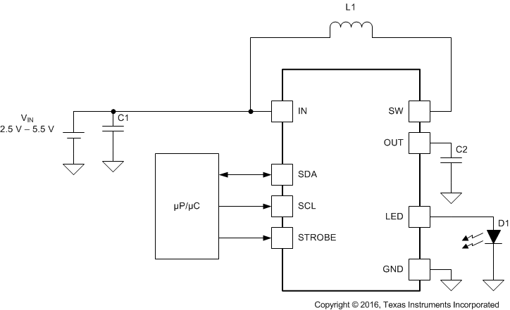
The LM36010 can drive a flash LED at currents up to 1.5 A. The 2-MHz or 4-MHz DC-DC boost regulator allows for the use of small value discrete external components.

Typical Application

LM36010 typicalapp.gif Figure 37. LM36010 Typical Application

Design Requirements

Example requirements based on default register values:

Table 1. Design Parameters

DESIGN PARAMETER EXAMPLE VALUE
Input voltage range 2.5 V to 5.5 V
Brightness control I2C Register
LED configuration 1 flash LED
Boost switching frequency 2 MHz (4 MHz selectable)
Flash brightness 1.5-A maximum current

Detailed Design Procedure

Thermal Performance

Output power is limited by three things: the peak current limit, the ambient temperature, and the maximum power dissipation in the package. If the die temperature of the device is below the absolute maximum rating of 125°C, the maximum output power can be over 6 W. However, any appreciable output current causes the internal power dissipation to increase and therefore increase the die temperature. Any circuit configuration must ensure that the die temperature remains below 125°C taking into account the ambient temperature derating. The thermal scale-back protection (TSB) helps ensure that temperature requirement is held valid. If the TSB feature is disabled, thermal shutdown (TSD) is the next level of protection for the device, which is set to 150°C. This mechanism cannot be disabled, and operation of the device above 125°C is not ensured by the electrical specification.

    In boost mode, where VIN < VLED + VHR, the power dissipation can be approximated by Equation 1:

    Equation 1. LM36010 pdiss_boost.gif

When the device is in pass mode, where VIN > VLED + VHR, the power dissipation equals:

Equation 2. LM36010 pdiss_pass.gif

Use Equation 3 to calculate the junction temperature (TJ) of the device:

Equation 3. LM36010 TJ.gif

Note that these equations only provide approximation of the junction temperature and do not take into account thermal time constants, which play a large role in determining maximum deliverable output power and flash durations.

Output Capacitor Selection

The LM36010 is designed to operate with a 10-µF ceramic output capacitor. When the boost converter is running, the output capacitor supplies the load current during the boost converter on-time. When the NMOS switch turns off, the inductor energy is discharged through the internal PMOS switch, supplying power to the load and restoring charge to the output capacitor. This causes a sag in the output voltage during the on-time and a rise in the output voltage during the off-time. Therefore, choose the output capacitor to limit the output ripple to an acceptable level depending on load current and input or output voltage differentials and also to ensure the converter remains stable.

Larger capacitors such as a 22-µF or capacitors in parallel can be used if lower output voltage ripple is desired. To estimate the output voltage ripple considering the ripple due to capacitor discharge (ΔVQ) and the ripple due to the capacitors ESR (ΔVESR), use Equation 4 and Equation 5:

For continuous conduction mode, the output voltage ripple due to the capacitor discharge is:

Equation 4. LM36010 deltaVQ.gif

The output voltage ripple due to the output capacitors ESR is found by:

Equation 5. LM36010 deltaESR.gifLM36010 deltaIL.gif

In ceramic capacitors, the ESR is very low so the assumption is that 80% of the output voltage ripple is due to capacitor discharge and 20% from ESR. Table 2 lists different manufacturers for various output capacitors and their case sizes suitable for use with the LM36010.

Input Capacitor Selection

Choosing the correct size and type of input capacitor helps minimize the voltage ripple caused by the switching of the boost converter and reduces noise on the input pin of the boost converter that can feed through and disrupt internal analog signals. In the typical application circuit a 10-µF ceramic input capacitor works well. It is important to place the input capacitor as close as possible to the LM36010 input (IN) pin. This reduces the series resistance and inductance that can inject noise into the device due to the input switching currents. Table 2 lists various input capacitors recommended for use with the LM36010.

Table 2. Recommended Input/Output Capacitors (X5R/X7R Dielectric)

MANUFACTURER PART NUMBER VALUE CASE SIZE VOLTAGE RATING
TDK Corporation C1608JB0J106M 10 µF 0603 (1.6 mm × 0.8 mm × 0.8 mm) 6.3 V
TDK Corporation C2012JB1A106M 10 µF 0805 (2 mm × 1.25 mm × 1.25 mm) 10 V
Murata GRM188R60J106M 10 µF 0603 (1.6 mm × 0.8 mm × 0.8 mm) 6.3 V
Murata GRM21BR61A106KE19 10 µF 0805 (2 mm × 1.25 mm × 1.25 mm) 10 V

Inductor Selection

The LM36010 is designed to use a 0.47-µH or 1-µH inductor. Table 3 lists various inductors and their manufacturers that work well with the LM36010. When the device is boosting (VOUT > VIN) the inductor is typically the largest area of efficiency loss in the circuit. Therefore, choosing an inductor with the lowest possible series resistance is important. Additionally, the saturation rating of the inductor must be greater than the maximum operating peak current of the LM36010. This prevents excess efficiency loss that can occur with inductors that operate in saturation. For proper inductor operation and circuit performance, ensure that the inductor saturation and the peak current limit setting of the LM36010 are greater than IPEAK in Equation 6:

Equation 6. LM36010 ipeak.gifLM36010 deltaIL.gif

where

  • ƒSW = 2 or 4 MHz

Efficiency details can be found in the Application Curves.
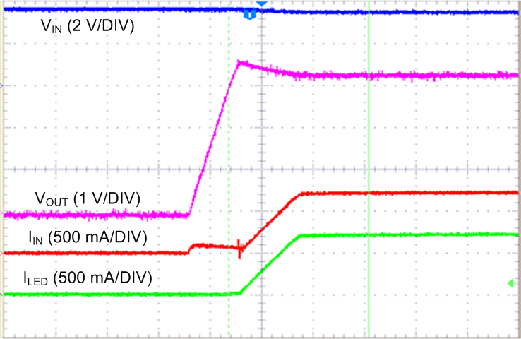
Table 3. Recommended Inductors

MANUFACTURER L PART NUMBER DIMENSIONS (L×W×H) ISAT RDC
TOKO 0.47 µH DFE201610P-R470M 2 mm × 1.6 mm × 1 mm 4.1 A 32 mΩ
TOKO 1 µH DFE201610P-1R0M 2 mm × 1.6 mm × 1 mm 3.7 A 58 mΩ

Application Curves
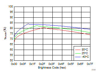
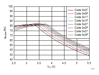
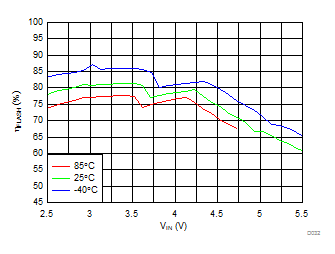
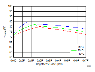
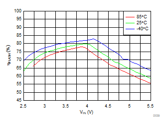
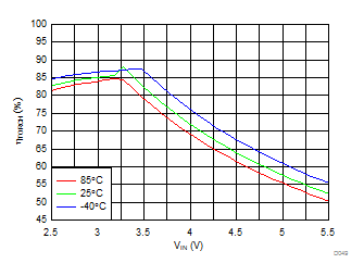
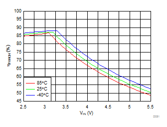
TA = 25°C, VIN = 3.6 V, CIN = 10 µF, COUT = 10 µF, L = 1 µH, VLED = 3.4 V, Flash Time-out = 320 ms and Thermal Scale-Back (TSB) disabled, unless otherwise noted.
LM36010 D028_SNVSAN4.gif
ƒSW = 2 MHz ICL = 2.8 A
Figure 38. LED Flash Efficiency vs Brightness Code
LM36010 D030_SNVSAN4.gif
ƒSW = 2 MHz ICL = 2.8 A
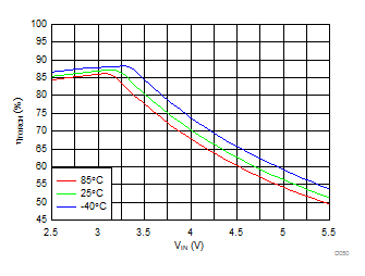
Figure 40. LED Flash Efficiency vs Input Voltage
LM36010 D032_SNVSAN4.gif
ƒSW = 2 MHz IFLASH = 1.5 A
ICL = 1.9 A Flash Time-out < 120 ms at 85°C
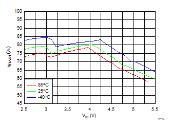
Figure 42. LED Flash Efficiency vs Input Voltage
LM36010 D034_SNVSAN4.gif
ƒSW = 2 MHz IFLASH = 1.2 A
ICL = 1.9 A Flash Time-out < 280 ms at 85°C
Figure 44. LED Flash Efficiency vs Input Voltage
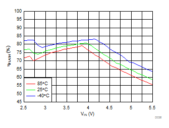
LM36010 D036_SNVSAN4.gif
ƒSW = 2 MHz IFLASH = 1.03 A ICL = 1.9 A
Figure 46. LED Flash Efficiency vs Input Voltage
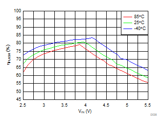
LM36010 D038_SNVSAN4.gif
ƒSW = 2 MHz IFLASH = 1.03 A ICL = 2.8 A
Figure 48. LED Flash Efficiency vs Input Voltage
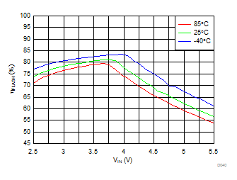
LM36010 D040_SNVSAN4.gif
ƒSW = 2 MHz IFLASH = 0.75 A ICL = 1.9 A
Figure 50. LED Flash Efficiency vs Input Voltage
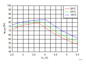
LM36010 D042_SNVSAN4.gif
ƒSW = 2 MHz IFLASH = 0.75 A ICL = 2.8 A
Figure 52. LED Flash Efficiency vs Input Voltage
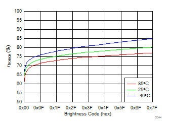
LM36010 D044_SNVSAN4.gif
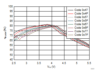
ƒSW = 2 MHz
Figure 54. LED Torch Efficiency vs Brightness Code
LM36010 D046_SNVSAN4.gif
ƒSW = 2 MHz
Figure 56. LED Torch Efficiency vs Input Voltage
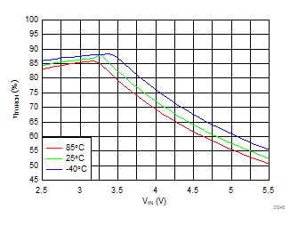
LM36010 D048_SNVSAN4.gif
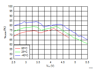
ƒSW = 2 MHz ITORCH = 376 mA
Figure 58. LED Torch Efficiency vs Input Voltage
LM36010 D050_SNVSAN4.gif
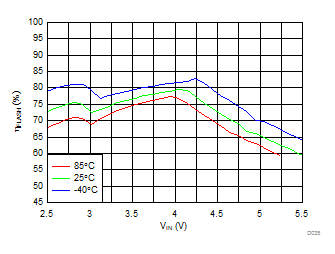
ƒSW = 2 MHz ITORCH = 258 mA
Figure 60. LED Torch Efficiency vs Input Voltage
LM36010 LM36010_scope_A01.png
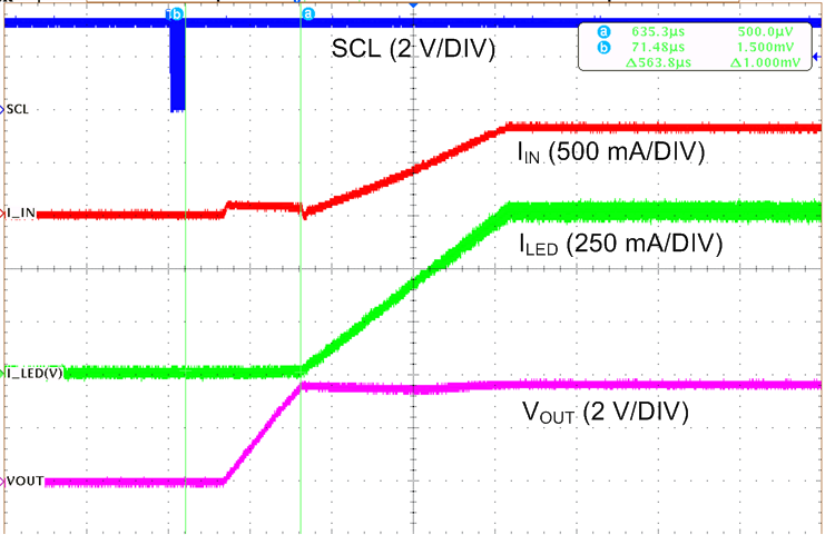
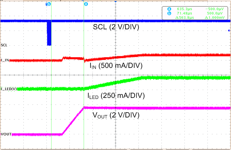
Time (400 µs/DIV)
Mode bits (Reg 0x01 bit[1:0]) = 11 (Flash Mode)
Figure 62. Flash Start-up with I2C
LM36010 LM36010_scope_A02b.png
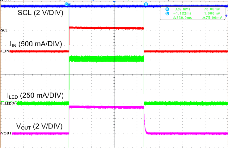
Time (2 ms/DIV)
Figure 64. Flash Turnoff with I2C
LM36010 LM36010_scope_A04.png
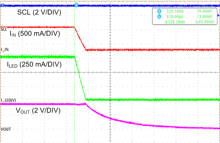
Time (4 ms/DIV)
Mode bits (Reg 0x01 bit[1:0]) = 00 (Standby Mode)
Figure 66. Torch Turnoff with I2C
LM36010 LM36010_scope_A06.png
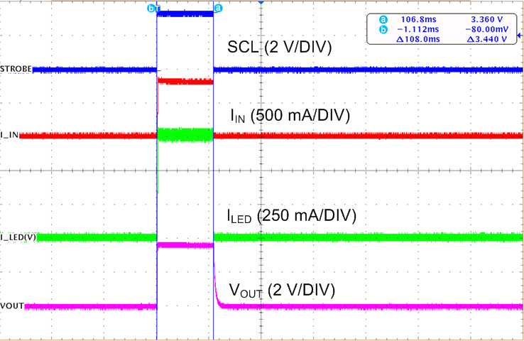
Time (100 ms/DIV)
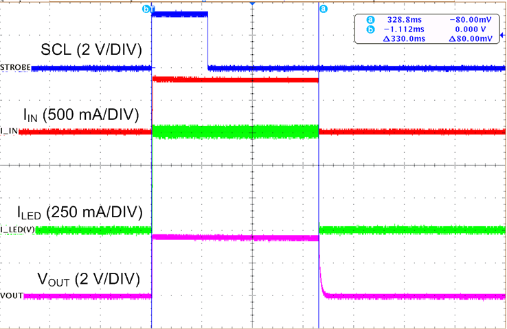
STROBE Enabled (Reg 0x01 bit[2] = 1)
Level Triggered (Reg 0x01 bit[3] = 0)
Strobe pulse = 100 ms
Figure 68. Flash Turnoff with Level Triggered STROBE
LM36010 LM36010_scope_A08.png
Time (400 µs/DIV)
Reg 0x01 = 0x26
Figure 70. Boost I2C Torch
LM36010 LM36010_scope_A10.png
Time (400 µs/DIV)
Reg 0x01 = 0x2C
Figure 72. Boost Edge Triggered Flash
LM36010 LM36010_scope_A12.png
Time (400 µs/DIV)
Reg 0x01 = 0xA6
Figure 74. Pass Mode I2C Torch
LM36010 LM36010_scope_A14.png
Time (400 µs/DIV)
Reg 0x01 = 0xAC
Figure 76. Pass mode Edge Triggered Flash
LM36010 LM36010_scope_A17.png
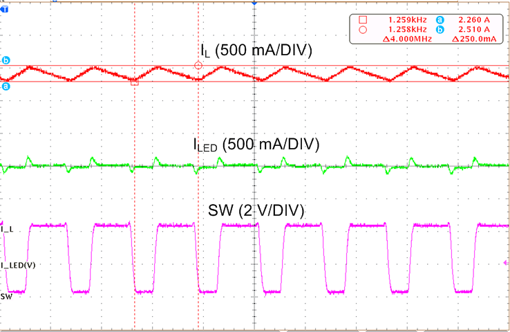
Time (200 ns/DIV)
ƒSW = 2 MHz
Figure 78. Inductor Current and Switch node (SW) Waveform
LM36010 LM36010_scope_A16.png
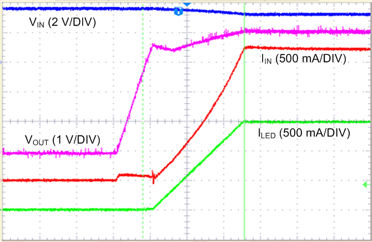
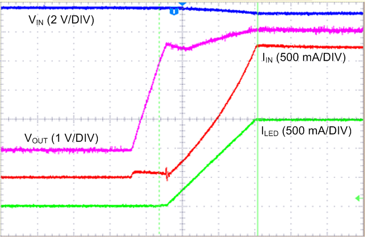
Time (400 µs/DIV)
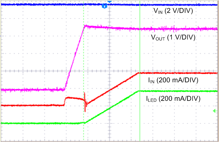
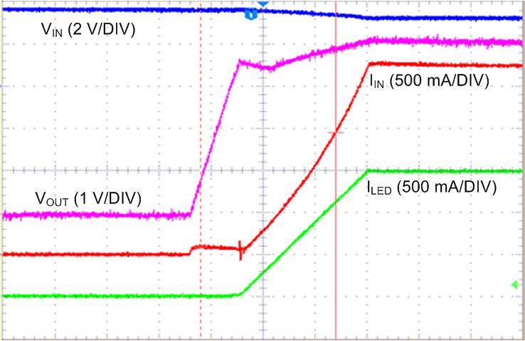
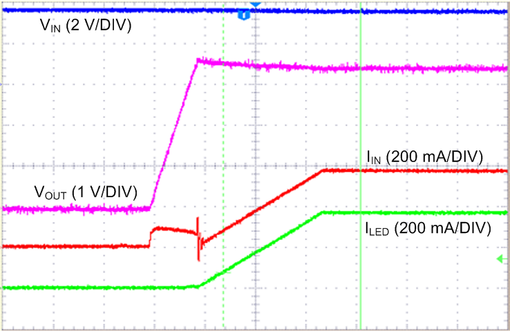
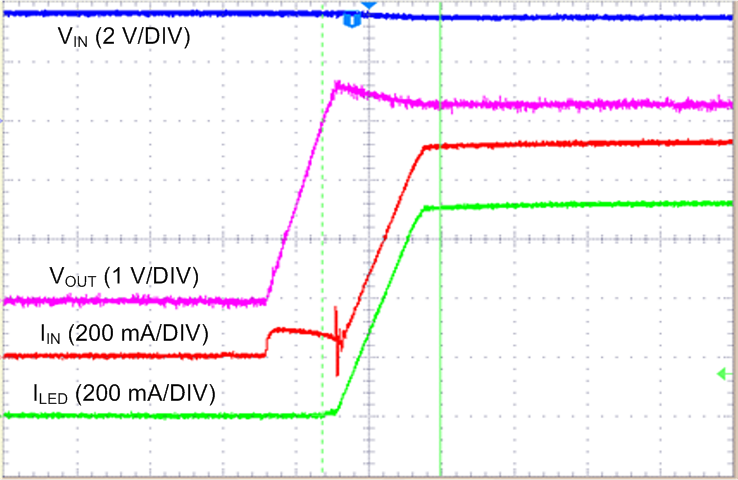
Reg 0x01 = 0x13 IVFM Trip Level (Reg 0x02 bits[7:5]) = 001 (3 V)
Figure 80. IVFM - Ramp and Hold
LM36010 D029_SNVSAN4.gif
ƒSW = 4 MHz ICL = 2.8 A
Figure 39. LED Flash Efficiency vs Brightness Code
LM36010 D031_SNVSAN4.gif
ƒSW = 2 MHz ICL = 2.8 A
Figure 41. LED Flash Efficiency vs Input Voltage
LM36010 D033_SNVSAN4.gif
ƒSW = 4 MHz IFLASH = 1.5 A
ICL = 1.9 A Flash Time-out < 120 ms at 85°C
Figure 43. LED Flash Efficiency vs Input Voltage
LM36010 D035_SNVSAN4.gif
ƒSW = 4 MHz IFLASH = 1.2 A
ICL = 1.9 A Flash Time-out < 280 ms at 85°C
Figure 45. LED Flash Efficiency vs Input Voltage
LM36010 D037_SNVSAN4.gif
ƒSW = 4 MHz IFLASH = 1.03 A ICL = 1.9 A
Figure 47. LED Flash Efficiency vs Input Voltage
LM36010 D039_SNVSAN4.gif
ƒSW = 4 MHz IFLASH = 1.03 A ICL = 2.8 A
Figure 49. LED Flash Efficiency vs Input Voltage
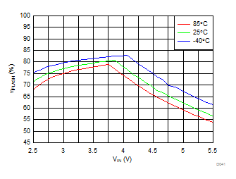
LM36010 D041_SNVSAN4.gif
ƒSW = 4 MHz IFLASH = 0.75 A ICL = 1.9 A
Figure 51. LED Flash Efficiency vs Input Voltage
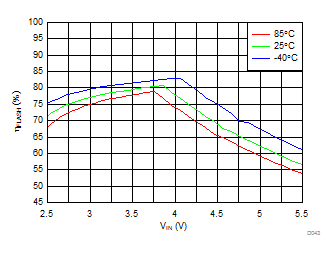
LM36010 D043_SNVSAN4.gif
ƒSW = 4 MHz IFLASH = 0.75 A ICL = 2.8 A
Figure 53. LED Flash Efficiency vs Input Voltage
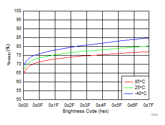
LM36010 D045_SNVSAN4.gif
ƒSW = 4 MHz
Figure 55. LED Torch Efficiency vs Brightness Code
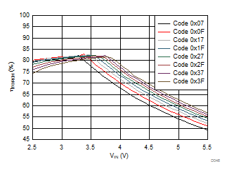
LM36010 D047_SNVSAN4.gif
ƒSW = 2 MHz
Figure 57. LED Torch Efficiency vs Input Voltage
LM36010 D049_SNVSAN4.gif
ƒSW = 4 MHz ITORCH = 376 mA
Figure 59. LED Torch Efficiency vs Input Voltage
LM36010 D051_SNVSAN4.gif
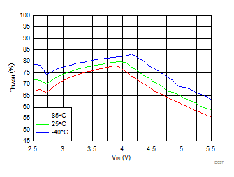
ƒSW = 2 MHz ITORCH = 188 mA
Figure 61. LED Torch Efficiency vs Input Voltage
LM36010 LM36010_scope_A02a.png
Time (100 ms/DIV)
Flash Time-out (Reg 0x02 bits[4:1]) = 0111 (320 ms)
Figure 63. Flash Time-Out
LM36010 LM36010_scope_A03.png
Time (400 µs/DIV)
Mode bits (Reg 0x01 bit[1:0]) = 10 (Torch Mode)
Figure 65. Torch Start-up with I2C
LM36010 LM36010_scope_A05.png
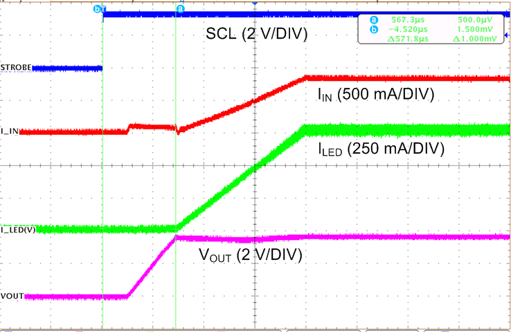
Time (400 µs/DIV)
STROBE Enabled (Reg 0x01 bit[2] = 1)
Figure 67. Flash Start-up with STROBE
LM36010 LM36010_scope_A07.png
Time (100 ms/DIV)
STROBE Enabled (Reg 0x01 bit[2] = 1)
Edge Triggered (Reg 0x01 bit[3] = 1)
Flash Time-out = 320 ms
Figure 69. Flash Turnoff with Edge Triggered STROBE
LM36010 LM36010_scope_A09.png
Time (400 µs/DIV)
Reg 0x01 = 0x27
Figure 71. Boost I2C Flash
LM36010 LM36010_scope_A11.png
Time (400 µs/DIV)
Reg 0x01 = 0x24
Figure 73. Boost Level Triggered Flash
LM36010 LM36010_scope_A13.png
Time (400 µs/DIV)
Reg 0x01 = 0xA7
Figure 75. Pass Mode I2C Flash
LM36010 LM36010_scope_A15.png
Time (400 µs/DIV)
Reg 0x01 = 0xA4
Figure 77. Pass mode Level Triggered Flash
LM36010 LM36010_scope_A18.png
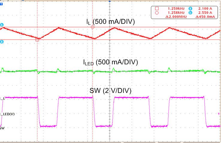
Time (200 ns/DIV)
ƒSW = 4 MHz
Figure 79. Inductor Current and Switch node (SW) Waveform