SNVSAN5A July 2017 – October 2017 LM36011
PRODUCTION DATA.
- 1 Features
- 2 Applications
- 3 Description
- 4 Revision History
- 5 Pin Configuration and Functions
- 6 Specifications
- 7 Detailed Description
- 8 Applications and Implementation
- 9 Power Supply Recommendations
- 10Layout
- 11Device and Documentation Support
- 12Mechanical, Packaging, and Orderable Information
Package Options
Refer to the PDF data sheet for device specific package drawings
Mechanical Data (Package|Pins)
- YKB|8
Thermal pad, mechanical data (Package|Pins)
Orderable Information
8 Applications and Implementation
NOTE
Information in the following applications sections is not part of the TI component specification, and TI does not warrant its accuracy or completeness. TI’s customers are responsible for determining suitability of components for their purposes. Customers should validate and test their design implementation to confirm system functionality.
8.1 Application Information
The LM36011 can drive a flash LED at currents up to 1.5 A. .
8.2 Typical Application
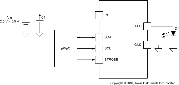 Figure 24. LM36011 Typical Application
8.2.1 Design Requirements
Example requirements based on default register values:
Table 1. Design Parameters
| DESIGN PARAMETER | EXAMPLE VALUE |
|---|---|
| Input voltage range | 2.5 V to 5.5 V |
| Brightness control | I2C Register |
| LED configuration | 1 flash LED |
| Flash brightness | 1.5-A maximum current |
8.2.2 Detailed Design Procedure
8.2.2.1 Thermal Performance
Output power is limited by two things: the ambient temperature, and the maximum power dissipation in the package. If the die temperature of the device is below the absolute maximum rating of 125°C, the maximum output power can be over 6 W. However, any appreciable output current causes the internal power dissipation to increase and therefore increase the die temperature. Any circuit configuration must ensure that the die temperature remains below 125°C taking into account the ambient temperature derating. The thermal scale-back protection (TSB) helps ensure that temperature requirement is held valid. If the TSB feature is disabled, thermal shutdown (TSD) is the next level of protection for the device, which is set to 150°C. This mechanism cannot be disabled, and operation of the device above 125°C is not ensured by the electrical specification.
The device power dissipation equals:

Use Equation 2 to calculate the junction temperature (TJ) of the device:

Note that these equations only provide approximation of the junction temperature and do not take into account thermal time constants, which play a large role in determining maximum deliverable output power and flash durations.
8.2.2.2 Input Capacitor Selection
Choosing the correct size and type of input capacitor helps minimize noise on the input pin of the boost converter that can feed through and disrupt internal analog signals. In the typical application circuit a 10-µF ceramic input capacitor works well. It is important to place the input capacitor as close as possible to the LM36011 input (IN) pin. This reduces the series resistance and inductance that can inject noise into the device. Table 2 lists various input capacitors recommended for use with the LM36011.
Table 2. Recommended InputCapacitors (X5R/X7R Dielectric)
| MANUFACTURER | PART NUMBER | VALUE | CASE SIZE | VOLTAGE RATING |
|---|---|---|---|---|
| TDK Corporation | C1608JB0J106M | 10 µF | 0603 (1.6 mm × 0.8 mm × 0.8 mm) | 6.3 V |
| TDK Corporation | C2012JB1A106M | 10 µF | 0805 (2 mm × 1.25 mm × 1.25 mm) | 10 V |
| Murata | GRM188R60J106M | 10 µF | 0603 (1.6 mm × 0.8 mm × 0.8 mm) | 6.3 V |
| Murata | GRM21BR61A106KE19 | 10 µF | 0805 (2 mm × 1.25 mm × 1.25 mm) | 10 V |
8.2.3 Application Curves
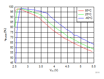
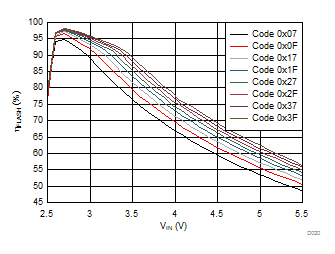
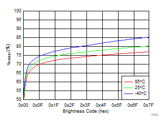
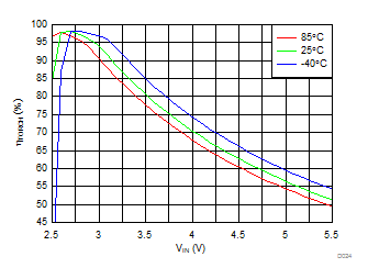
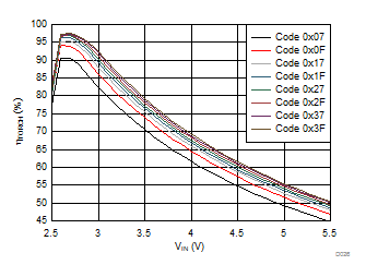
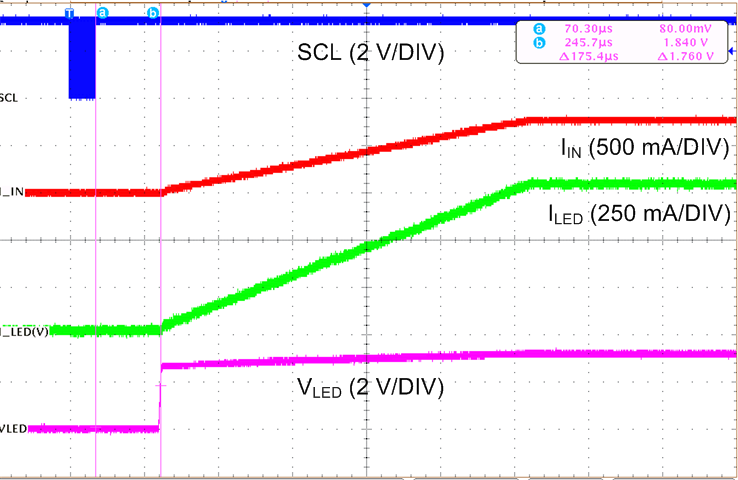
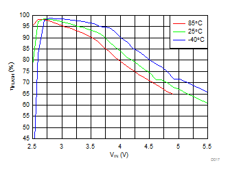
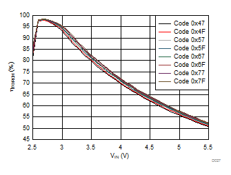
TA = 25°C, VIN = 3.6 V, CIN = 10 µF, VLED = 3.4 V, Flash Time-out = 320 ms and Thermal Scale-Back (TSB) disabled, unless otherwise noted.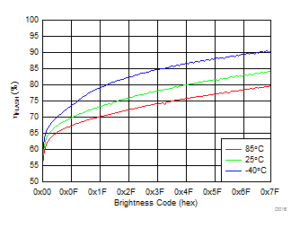
| VIN = 4.0 V |
| IFLASH = 1.03 A | ||
| ITORCH = 258 mA | ||
| Time (200 µs/DIV) | ||
| Mode bits (Reg 0x01 bit[1:0]) = 11 (Flash mode) |
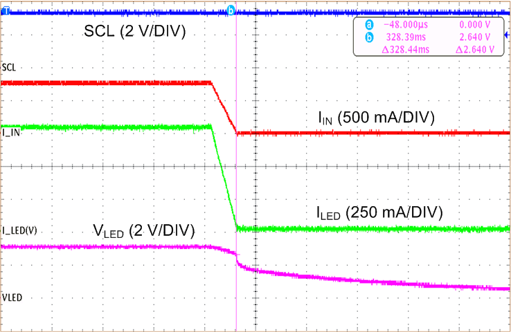
| Time (2 ms/DIV) |
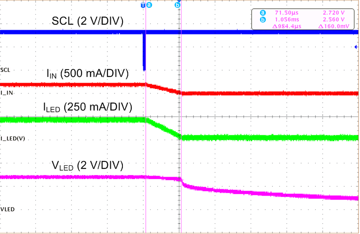
| Time (1 ms/DIV) | ||
| Mode bits (Reg 0x01 bit[1:0]) = 00 (Standby mode) |
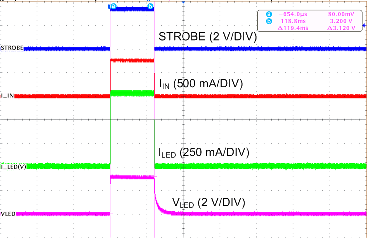
| Time (100 ms/DIV) | ||
| STROBE Enabled (Reg 0x01 bit[2] = 1) | ||
| Level Triggered (Reg 0x01 bit[3] = 0) | ||
| Strobe pulse = 100 ms |
| IFLASH = 1.5 A | ||
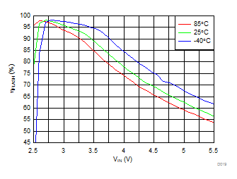
| IFLASH = 0.75 A | ||
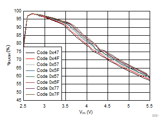
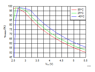
| ITORCH = 376 mA | ||
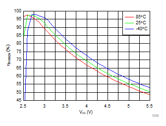
| ITORCH = 188 mA |
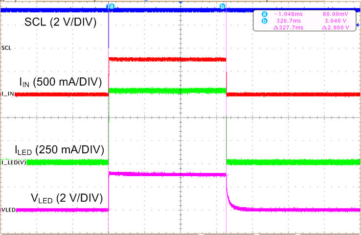
| Time (100 ms/DIV) | ||
| Flash Time-out (Reg 0x02 bits[4:1]) = 0111 (320 ms) |
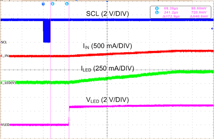
| Time (200 µs/DIV) | ||
| Mode bits (Reg 0x01 bit[1:0]) = 10 (Torch mode) |
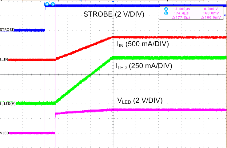
| Time (400 µs/DIV) | ||
| STROBE Enabled (Reg 0x01 bit[2] = 1) |
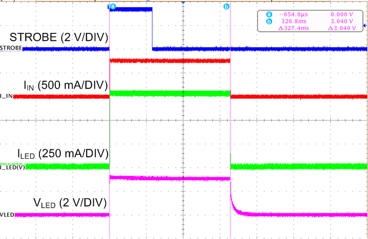
| Time (100 ms/DIV) | ||
| STROBE Enabled (Reg 0x01 bit[2] = 1) | ||
| Edge Triggered (Reg 0x01 bit[3] = 1) | ||
| Flash Time-out = 320 ms |