SNVS891H September   2012  – September 2015 LM3642

PRODUCTION DATA.  

  1. Features
  2. Applications
  3. Description
  4. Revision History
  5. Pin Configuration and Functions
  6. Specifications
    1. 6.1 Absolute Maximum Ratings
    2. 6.2 ESD Ratings
    3. 6.3 Recommended Operating Conditions
    4. 6.4 Thermal Information
    5. 6.5 Electrical Characteristics
    6. 6.6 Timing Requirements
    7. 6.7 Typical Characteristics
  7. Detailed Description
    1. 7.1 Overview
    2. 7.2 Functional Block Diagram
    3. 7.3 Feature Description
      1. 7.3.1 Power Amplifier Synchronization (TX/TORCH)
      2. 7.3.2 Input Voltage Flash Monitor (IVFM)
      3. 7.3.3 Fault and Protections
        1. 7.3.3.1 Fault Operation
        2. 7.3.3.2 Flash Time-Out
        3. 7.3.3.3 Overvoltage Protection (OVP)
        4. 7.3.3.4 Current Limit
        5. 7.3.3.5 Undervoltage Lockout (UVLO)
        6. 7.3.3.6 Thermal Shutdown (TSD)
        7. 7.3.3.7 LED and/or VOUT Fault
    4. 7.4 Device Functional Modes
      1. 7.4.1 Start-up (Enabling the Device)
      2. 7.4.2 Pass Mode
      3. 7.4.3 Flash Mode
      4. 7.4.4 Torch Mode
      5. 7.4.5 Indicator Mode
    5. 7.5 Programming
      1. 7.5.1 I2C-Compatible Interface
        1. 7.5.1.1 Data Validity
        2. 7.5.1.2 Start and Stop Conditions
        3. 7.5.1.3 Transferring Data
        4. 7.5.1.4 I2C-Compatible Chip Address
        5. 7.5.1.5 Transferring Data
    6. 7.6 Register Map
      1. 7.6.1 Register Descriptions
        1. 7.6.1.1 Enable Register (0x0A)
        2. 7.6.1.2 Flags Register (0x0B)
        3. 7.6.1.3 Flash Features Register (0x08)
        4. 7.6.1.4 Current Control Register (0x09)
        5. 7.6.1.5 Input Voltage Flash Monitor (IVFM) Mode Register (0x01)
        6. 7.6.1.6 Torch Ramp Time Register (0x06)
        7. 7.6.1.7 Silicon Revision Register
  8. Application and Implementation
    1. 8.1 Application Information
    2. 8.2 Typical Application
      1. 8.2.1 Design Requirements
      2. 8.2.2 Detailed Design Procedure
        1. 8.2.2.1 Output Capacitor Selection
        2. 8.2.2.2 Input Capacitor Selection
        3. 8.2.2.3 Inductor Selection
      3. 8.2.3 Application Curves
  9. Power Supply Recommendations
  10. 10Layout
    1. 10.1 Layout Guidelines
    2. 10.2 Layout Example
  11. 11Device and Documentation Support
    1. 11.1 Device Support
      1. 11.1.1 Third-Party Products Disclaimer
    2. 11.2 Documentation Support
      1. 11.2.1 Related Documentation
    3. 11.3 Trademarks
    4. 11.4 Community Resources
    5. 11.5 Electrostatic Discharge Caution
    6. 11.6 Glossary
  12. 12Mechanical, Packaging, and Orderable Information

Package Options

Mechanical Data (Package|Pins)
Thermal pad, mechanical data (Package|Pins)
Orderable Information

1 Features

  • 1.5-A High-Side Current Source for Single LED
  • > 85% Efficiency in Torch Mode (at 100 mA) and Flash Mode (at 1 A to 1.5 A)
  • Accurate Programmable Flash LED Current from 93 mA to 1.5 A
  • Accurate Programmable Torch LED Currents:
    • 48.4 mA to 375 mA
    • 24 mA to 187 mA (LT option)
  • Small Solution Size: < 20 mm2
  • Soft-Start Operation for Battery Protection
  • Hardware Strobe Enable
  • Synchronization Input for RF Power Amplifier Pulse Events
  • VIN Flash Monitor Optimization
  • 400-kHz I2C-Compatible Interface
  • 0.5-mm Pitch, 9-Bump DSBGA

2 Applications

    Camera Phone LED Flash

3 Description

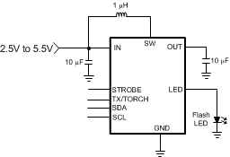
The LM3642 is a 4-MHz fixed-frequency synchronous boost converter plus 1.5-A constant current driver for a high-current white LED. The high-side current source allows for grounded cathode LED operation providing Flash current up to 1.5 A. An adaptive regulation method ensures the current source remains in regulation and maximizes efficiency.

The LM3642 is controlled via an I2C-compatible interface. Features include a hardware flash enable (STROBE) allowing a logic input to trigger the flash pulse as well as a TX input which forces the flash pulse into a low-current Torch Mode, allowing for synchronization to RF power amplifier events or other high-current conditions.

The 4-MHz switching frequency, overvoltage protection and adjustable current limit settings allow the use of tiny, low-profile inductors and (10-µF) ceramic capacitors. The device is available in a small 9-bump DSBGA package and operates over the −40°C to 85°C temperature range.

Device Information(1)

PART NUMBER PACKAGE BODY SIZE (MAX)
LM3642 DSBGA (9) 1.69 mm × 1.64 mm
  1. For all available packages, see the orderable addendum at the end of the data sheet.

Simplified Schematic
LM3642 30178901.gif